This thread has been locked.

If you have a related question, please click the "Ask a related question" button in the top right corner. The newly created question will be automatically linked to this question.

UCC256301: How to set optocoupler current in UCC2560X feedback chain.

Part Number: UCC256301
Other Parts Discussed in Thread: UCC25630-1EVM-291, TLVH431, ATL431, TL431, UCC25600

The feedback chain of UCC25630X EVM schematic is shown below.

1. how to set the optocoupler LED forward current (IF)?

2. how to select R23, if the output voltage is 24V.?

3. what the function of R20?

The CTR value of the optocoupler VO618A-3, is 100%-200%,  so the current flow from FB pin to PGND is 100%-200% of IF, the rough value of IF i calculated is about (Vout-Vled-Vref)/R23=(12-1-1.24)/6k=1.6mA.

However, the internal current source IFB at FB pin, is only 85uA,  which is much smaller than the current flow from FB pin to PGND.

4. How to explain my calculation result?

By the way.

5. what's the function of the D10 and R21 shown on the picture.

  • Hello Shubiao,

    Let me answer your questions out of order to get the simpler ones out of the way.

    For Q5: The function of D10 and R21 is explained in section 5.2 of the UCC25630x Practical Design Guidelines document (www.ti.com/.../slua836a.pdf ). It is used to avoid optocoupler saturation which could transient response.

    For Q3: R20 is used to provide bias current to the shunt regulator when IFB is near zero and the photo diode current is negligible. When significant current flows through the photo diode, it typically generates about 1~1.2 V across it. To cut off IFB, the photo diode current must also decrease to near zero. However the shunt regulator still needs bias current to continue to operate properly. It is common to place a resistor across the diode to provide the bias current to the shunt regulator. The diode can still have 0.5~0.6 V across it while having negligible current through it. This 0.5V is applied across R20 used to provide the minimum current needed by the regulator. The TL431 requires at least 400 uA, but worst-case up to 1 mA to operate. For this part, a 500-ohm bias resistor would be necessary. The UCC25630-1EVM-291 uses a TLVH431 which needs only 100 uA to operate. Here 0.6V/100uA = 6 Kohm bias resistor for R20. In general, the value of the bias resistor (R20 on the EVM) depends on the minimum current that the specific shunt regulator that is used in a specific design. (For a 24-V output, the TLVH431 regulator is not appropriate because it is rated for only 20 V. However, an ATL431 is a low-bias device suitable for a 24-V output, for example.)

    For Q1: The optocoupler IF is set by the required collector current on the output. In this case, the collector current (which is IFB) is limited to the range between 0 uA and 85 uA (typ). One must look at the optocoupler CTR curves to determine the actual CTR at the bias level actually applied. Figure 13 of the VO618A datasheet indicates that non-saturated CTR at IF = 100 uA (at 25C) is about 20% of the rated CTR. The EVM uses VO618A-3 which is rated for 100%-200% CTR at IF = 1 mA, Vce = 5V. From these curves one can deduce that to drive IFB = 85 uA, IF must be about 243 mA (~35% of 100% of 1mA) at 25C and IF must be higher at higher ambient temperatures.

    For Q4: As explained in the answer to Q3, the nominal CTR rating does not hold at low collector currents. CTR drops considerably at uA levels. Furthermore, the shunt regulator will adjust its cathode voltage up and down to achieve the IF required to keep the output voltage regulated under the varying line and load conditions. So the voltage across R23 will not be (Vout-Vled-Vref), but will be (Vout-Vled-Vcathode) and the regulator can adjust Vcathode up quite close to Vout in order to achieve the correct amount of current through R23 and ultimately through the photo diode.

    For Q2: The maximum value for R23 is determined by the IF current needed to achieve 85uA with the shunt regulator is saturated. In this case, IF may = ~350 uA when hot (~24% at 110C ambient). Add 1V/6K = 167 uA bias current through R20 for a total of 517 uA cathode current. This needs to be generated even if the shunt regulator is saturated on, so R23 < (24V – 1V - ~2V)/517uA = 40.6 Kohm max.
    But the actual value will be lower than that and it factors into the loop gain needed for loop stability.
    The minimum value is such as to prevent overstress to the diode and shunt. 5 mA is sufficient, so R23 must be > ~4 Kohm minimum.
    I don’t have a reference to loop-compensation design at the moment. I’ll search for this information and provide it in a follow-on reply as soon as I can (tomorrow, I hope).

    Does this answer your questions?

    Regards,
    Ulrich
  • Thanks Ulrich,

    This helps a lot .

    for the loop-compensation design. i have read a reference about how to design loop compensation based on UCC25600. 

    However, the UCC25630x has a totally different transfer function with UCC25600. furthermore, the IFB in UCC25630x feedback chain also has difference with that in UCC25600.

    Do you have any similar analysis on UCC25630x loop design and compensation as mentioned above.

    BRs, Shubiao

  • Hello Shubiao,

    I will inquire with the experts about any non-published specific compensation guide for the UCC25630x series.  Otherwise, everything that I have access to is also on the TI website in these parts' product folders, under the "Technical Documents" tab.

    Because of the holidays, a response may be delayed.

    Regards,
    Ulrich

  • Thanks Ulrich,

    hope to get the compensation guide for the UCC25630X after the holidays.

    Regards!
    Shubiao
  • Hello Shubiao,

    Here is an update on the status of your request.
    The expert that I rely on is still out on holiday this week. I expect him to return next Monday Jan 7th and I'll be able to ask him for the information then.

    Regards,
    Ulrich
  • Thanks a lot Ulrich,

    Happy new year to you!
    Shubiao
  • Hello Shubiao,


    Here is the advice that I obtained concerning loop compensation for the UCC25630x:


    The transfer function is slightly different because of the inner charge control loop on the primary side. There is no closed-form solution for the transfer function yet, unfortunately.  Hybrid Hysteretic Control (HHC) is similar to bang-bang charge control presented in a paper by researchers at Queens University in Canada, but the transfer function presented in the paper does not include the frequency compensation ramp current that is added to make HHC. A comparison between conventional direct frequency control and HHC shows that a complex-pole response is replaced by a single-pole response, which is easier to compensate.


    There isn’t an official guideline for compensation at the moment for UCC25630x devices. Generally, most designs use type-II with a zero placed in the general vicinity of 1/(2*pi*Rload*Cout), and a pole placed a few kHz after the desired crossover frequency to roll off the gain. This is just a “fast and loose” rule however so it is not sufficient to be considered “official” guidance.


    The design guide for the UCC25600 (mentioned above) is still relevant for UCC25630x compensation. This approach will also work.


    Additional guidance provided to me is:


    Since there is no accurate mode of HHC LLC, there are some experimental design considerations for the secondary side circuit as follows:

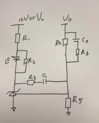
    The circuit structure is shown as below

    1.  R6 and C2 is not necessary

    2.  Zero point of R3 and C1 is below 100Hz, which is helpful for burst mode overshoot

    3.  R5 should larger than 2kohm

    4.  Initial gain should larger than 30dB

    Test gain/phase curve firstly, then adjust components in above picture to meet the target specs.


    Regards,

    Ulrich

  • Thanks Ulrich, 

    You professional comments helps a lot.

    • regarding on the: 2.  Zero point of R3 and C1 is below 100Hz, which is helpful for burst mode overshoot; I believe the Zero point here is 1/((R3+R4)*C1*2*Pi), that means the R4 has great effort on the zero point.

    Shubiao

  • Hi Shubiao,

    Actually, R4 plays no part in the zero frequency, and R3 plays no part in the pole.
    Consider that internal to the TL431, R3 + C1 are a feedback impedance from the output of an op-amp to its negative input (the REF input), considered to be a virtual AC-GND.
    By classic op-amp theory with infinite gain and bandwidth, Vo/Vin gain = Zf/Zin. Zf = R3 + X1, Zin = R4. X1 = 1/sC1.
    (R6 and C2 are not used. If they were included, Zin would become more complex.)

    So, Vo/Vin = (R3 + 1/sC1) / R4 = ((sC1R3 + 1)/sC1) / R4 = (sR3C1 +1) / sR4C1.
    This gain curve has a pole at dc (0 Hz), a -1 down-slope (-20dB/decade), and a zero at 1/2piR3C1. R4 does not affect the zero.
    R4 would determine where the 0dB crossover frequency (gain = 1/1) would be if R3 = 0.

    In reality, the TL431 op-amp has limited gain and finite bandwidth, but as long as the -1 slope crossover and the zero frequency are low enough, those equations are reasonable approximations not significantly affected by the TL431 limitations.
    Note: this applies to any similar shunt-regulator or error-amp configuration, not just the TL431.

    Regards,
    Ulrich
  • Ulrich,

    The target small signal transfer function here is Iled/Vout, not just Vtl431/Vout; 

    (By the way, i believe you miss a minus sign in the transfer function of Vtl431/Vout, it should be" -(sR3C1 +1) / sR4C1", R6 and C2 are not used.)

    Iled/Vout= (Vout-Vtl431)/R1= (Vout+ Vout*(sR3C1 +1) / sR4C1))/R1; 

    Thus, the transfer function will be derived to Lled/Vout= s(R3+R4)C1/(sR1R4C1).

    Shubiao

  • Hello Shubiao,

    You are right; I missed the minus sign.
    Also, I agree that extending the function to the LED current will result in the (R3+R4)C1 zero as your calculations show.

    Thanks for making that point clear.
    I believe the difference depends on whether R1 is fed by a fixed 12V source or from Vout. I believe that tying R1 to Vout causes the zero to include R4 and R3 because loop perturbations will affect both inputs (at R1 and at R4) to the LED current.

    I will relay this difference in approach back to the LLC engineering team, to clarify their procedures.

    Regards,
    Ulrich