This thread has been locked.

If you have a related question, please click the "Ask a related question" button in the top right corner. The newly created question will be automatically linked to this question.

UCC28070

Other Parts Discussed in Thread: UCC28070, UCC27324, UCC28019, THS4281

Hi,


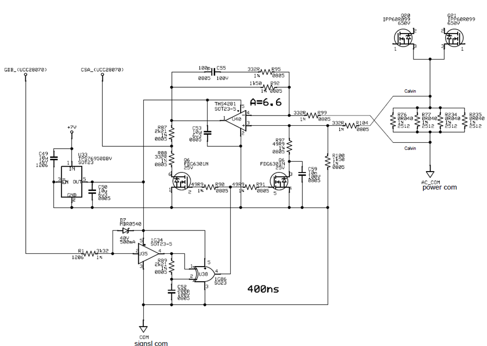
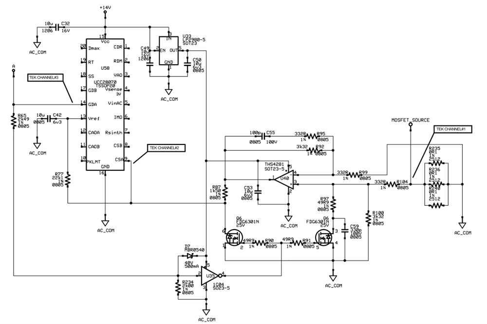
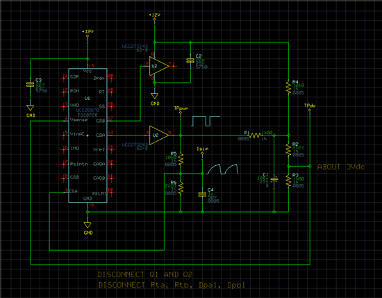
I am actually designing a 3,3  kW PFC for a Battery Charger and have some problems with the PFC-IC.

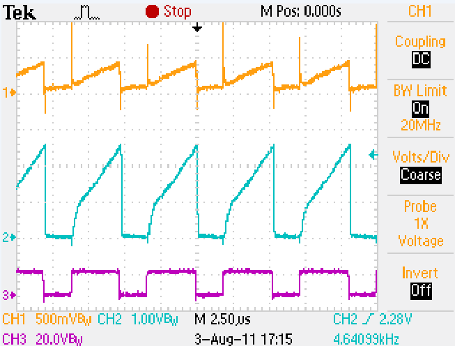
The reference voltage varies between 5,8 and 6,3 V dependend on the VINAC voltage. GDA and GDB give no signal out as long as there is an AC Power Supply. As soon as I switch off the AC Power Supply and the VSENSE voltage is still over 0,75 V the GDA output is working on maximum duty cycle. Of course the Mosfet doesn't switch because there is no AC input. The GDB doensn't work at all. As soon as there comes a minimal VINAC voltage the GDA stops working as well.


Can somebody help?


Regards, Otto Kreutzer

  • Otto. Hi,

    If you give more details about your schematic. For example: How you power up UCC2870...what frequency you choose ...current sensors....input voltage...output voltage...some details about PCB design ...magnetics and so,we can work on this problem.

    Dragan

  • Hi Dragan,

    thanks a lot for your answer.

    I already tried a lot. The change of the reference voltage was a defect of the IC. I changed now the controller and the reference voltage stays now on 6 V.

    Just to describe the problem again after the change of the controller:

    As long as I keep the current sense (CSA and CSB) on ground and no current flows over the Mosfets (Input power +230 V must be turned off) the Mosfet outputs give out the maximum duty cycle. As soon as I put there a small Input voltage (beginning at 1-2 V) at the +230 V input the Mosfet outputs GDA and GDB swith off immediately (Output capacitator must be charged to keep the VSENSE over 0,75 V).

    What I wonder is that the UCC28070 has no information any more whether current flows or not. The CSA and CSB inputs are connected to ground. I also switched the current synthesis off without any effect.
    I also generated the VINAC signal with a signal generator without any effect.
    I also tried to measure the current signal with a resistor between Mosfet source and ground and supply the CSA and CSB with that signal. The only result I got was that the duty cycle of GDA and GDB went down on 1-3 %.
    I attached the Excel spreadsheet and the schematic.
    Best regards,
    Otto Kreutzer
    SCHEMATIC UCC28070.pdf
  • Hi Otto,

     - Rb22 and Rb12 ( 1R) resistors and should be removed.

      - Rta and Rtb (430R) is too big  load for GDA and GDB outputs so move GDA and GDB "Mosfet Treiber Strommessteil" input to the U1 (UCC27324) pin 7 and 5.  

      -Remove D4 and D5

    Dragan


  • Hi Dragan,

    thank you for your reply.

    RB12 and RB22 are not used, I just added them for the board layout to be able to adjust RB11 and RB21 if necessary. Sorry that I didn't tell you before.

    Thanks a lot for the idea to connect the "Mosfet Treiber Strommessteil" to the output of the Mosfet driver. I tried it out, but unfortunately it brought no improvement.

    I also removed D4 and D5.

    Just for your information:

    Rsynth and CDR are connected to Vref and Rrdm is connected to ground to disable the current synthesis and the frequency dithering.

    I already soldered out the whole Mosfet Treiber Strommessteil to test without any Current input for the UCC28070.

    I removed for testing reasons the CB11, DB12, CB21 and Cb22. No effect.

    I also removed the Cs1,Cs2,Cs3. No effect.

    As soon as I exchange the L1 and L2 with a resistor the UCC28070 and the Mosfets keep working on maximum duty cycle. As soon as I add any inductor the GDA and GDB is disabled again.


    Thanks for your help ,


    Otto Kreutzer


  • Hi,

    Here is small schematic ,easy to apply in existing circuit tree, can help to simulate  proper work of controller . Playing with values of R6 and C4 you can check current limit and

    allso  with R3 output voltage.

    Dragan


    .

  • Hi Dragan,

    thanks for your answer.

    It's quite hard to read the values in your schematic because of the low resolution. If you could send the picture in a higher resolution I would be glad. My Email is Otto.Kreutzer@qestronic.de

    Anyway, I am actually in contact with an TI engineer, and he asked me to do some measurement when the controller is ramping up.

    I uploaded them for you as well.

    One can see clearly, that the controller resets every 30 ms as soon as there is an VINAC voltage. Why he does that, I don't know yet. Maybe you can help.

    I exchanged the controller again. After that the phenomen with the maximum duty cycle doesn't show up any more.

    Thank you,

    Otto Kreutzer

    Signals.zip
  • hi otto

    i have the same problem as i turn off 230v AC it start to generate gate pulses but as i turned it on again it stop working.i also have a problem that first it was generating 450v at out put according to my requirement but when i put load voltage drops to 300v .and now it is not giving 450v out it only give 310v out do u have  any idea what problem it could be.

    Best Regards 

    Muhammad Farhan Alam

  • Dear Muhammad,

    I tried to get my board running from Mid of March to Mid of June. Since I am working quite close to the European headquater of TI, I brought my board to the TI support and it stayed there for 3 weeks. They didn't find the mistake as well, they just told me general improvements.

    After those three months I gave up and changed the controller to the ÚCC28019. By the way, I am building a 3,3 kW car charger as well. The UCC28019 works perfectly even up to 3,3 kW. Unfortunately the ripple currents are far higher and the inductors are bigger as well, since it is a one phase controller and has no sync pin to switch more controllers together.

    Since TI didn't get the controller running themselves, our next step is to build the charger with a 2-phase PFC controller of a competitor. Our actual plan is a Fairchild controller.  We would like to test it with a 4-phase controller as well to reduce the space of the PFC.

    Which company are you designing the car charger for?

    Regards,

    Otto

  • hi

    Dear otto 
    i am doing my master at Mid Sweden university (Sweden) this is a part of my thesis work.but now as u say that TI them self's are not able  to run it this is not good new .but thanks very much for your detail answer.
    Thanks
    Best Regards
    Muhammad Farhan Alam   

  •  

    hi Dragan

    we have been working with the PFC using 3.3 kw it is performing the function but the out put voltage starts to decrease as we put load and then never recovers .we are not sure about the current sense signals at CSB and CSA pins how the wave form should be .i have attached the picture in which yellow is the wave form at current transformer and blue is the curve at CSB pin but its looks that nothing is on CSB can any one explain that how the signal should be on CSB and CSA

  • Hi Imran,


    I am using this circuit for current sensing. Beside THS4281 (HS amplifier) are 1G34 and 1G86 in function to suppress noise  during OFF time. Working grate on 250kHz. Identical circuit is on  CSB side. It is not simple like transformer  but works better.  I hope I have working prototype in lab. and I am going to record all waveforms on UCC28070.

    Dragan

  • Irman,

    This is Schematic and w.f.

    Dragan


  • dear dragan

    thanks for your fast reply. i will try this and hope it will work... 

    best regards

    imran