This thread has been locked.

If you have a related question, please click the "Ask a related question" button in the top right corner. The newly created question will be automatically linked to this question.

TPS543C20: Current rating recommendations according to VIN

Part Number: TPS543C20
Other Parts Discussed in Thread: , TPS543B20

Hello,

My customer found the current rating recommendations on the TPS543C20 datasheet as below.

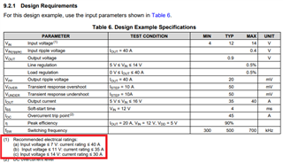
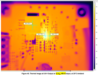
The test results for 40A at 12Vin are also in the datasheet as follows:

Why are there recommended current ratings?

Are these recommendations mandatory for TPS543C20 users to follow? 

What problems can be expected if the recommended current rating according to the input voltage is not observed?

Thank you.

JH

  •  

    The recommended Current verse PVIN voltage are intended to protect the high-side and low-side devices from excessive voltage stress, especially PVIN to SW during the turn-off of the high-side FET.  As long as the PVIN to to SW and SW to PGND voltage stress ratings are met, it is possible to exceed the listed current levels, but when exceeding the listed current levels designers should very carefully analyze these dynamic voltage stresses.

  • Hi Miller,

    Thanks for your reply.

    The customer downloaded the simulation file below from TI webench as the TPS543C20A.

    (TPS543C20 is not supported by TI webench)

    WBDesign80_Load Transient-7.pdf

    Is there any problem with using the TPS543C20 under the same conditions?

    Thank you.

    JH

  • To operate the TPS543C20 at 35A from a 13V input safely, you will need to have careful layout of the power input bypassing and its return to the thermal pad ground.  I would also recommend including a SW to PVIN snubber (instead of a typical SW to PGND snubber)  The SW to PVIN snubber will reduce the PVIN to SW stress during the turn-off of the low-side FET more than a SW to GND snubber would.

    I would also recommend including two 4.7nF or 6.8nF 0402 capacitor placed on the backside of the PCB under the PVIN pins between PVIN and PGND at the thermal pad. with vias placed as close to the PVIN pins  as design rules allow.  This capacitor, which has a self-resonant frequency of about 100MHz will help dampen the switch transition stress on PVIN and reduce the PVIN to SW stress during the turn-off of the high-side FET.

  • Hi Peter,

    Thanks for your help.

    Could you please review the schematic and artwork of the TPS543C20 to ensure it is properly designed as your guide? 

    TPS543C20RVFR_Review.pdf

    Thank you.

    JH

  •  

    Please see the TPS543B20 TPS543C20A TPS543C20 Excel Calculator Tool and Checklist in the TPS543C20 product folder under Design & Development and Design Tools and Simulation - https://www.ti.com/product/TPS543C20#design-tools-simulation 

    It includes a design tool as well as well as the schematic and layout checklists.  If you have specific questions or concerns after reviewing your schematic or design, we can review those.

  • Hi Peter,

    Please review the circuit and artwork for SW to PVIN Snubber and PSN/PSP applied by the customer to reduce PVIN stress.

      - 1nF/50V/1005 CAP and 2ohm/1%/105 RES were used as Snubber.

      - For RSN/RSP circuit, the values confirmed in Webench were applied.

    Please check whether the remote sensing trace length is a problem.

    Thank you.

    JH

  •  

    The power dissipation in the snubber resistor for 12V @ 500kHz with a 1nF capacitor is about 72mV, which is greater than the 1/16W rating of a 1005 (0402) resistor, so I would definitely recommend selecting at least an 1608 (0603) 1/10W resistor package.

    I would recommend additional ground vias for C475, C476, and C477 to be most effective.  While their in-pad via is good, only 1 via per capacitor is somewhat limiting.

    If there is space to place the 6.8nF capacitor on the back side of the board with vias to VIN and direct connection to the backside of the thermal pad via array, that would be even better for switch node ringing reduction.

    Regarding the Remote Sense lines:  Am I reading slides correctly that they are approximately 150mm (6 inches) ?  That appears to be quite long, and likely to introduce a power-path pole due to the distribution inductance and remote bypass capacitance, so I would recommend adding a capacitor from output voltage close to L4 back to net between R415 and R417 that could be used to counter that added pole at high frequency and improve loop stability,

    Providing 2 vias to bring the SW node to the backside of the PCB for the GND and PVIN snubbers, as well as 2 vias for connecting them to VIN and GND  would also help reduce their loop inductance.

    I would also recommend narrowing the SW area from the TPS543C20 to L4. 

    Other wise, I think things look good.