This thread has been locked.

If you have a related question, please click the "Ask a related question" button in the top right corner. The newly created question will be automatically linked to this question.

TPS650861: Buck 2 not working

Part Number: TPS650861
Other Parts Discussed in Thread: MSP430F5529,

Hi Team,

Customer is facing turn ON issue with Buck 2 output, device provides 0.14V instead of 1V.

Attached are the waveforms on high and low side gate drive nodes. The gate drive nodes are always with 5V level,  switch node is staying at “0” with some spurious spike.

Looks like drive high is not going to required level. The behavior remains same with Full load and no load condition.
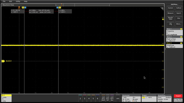
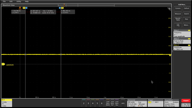
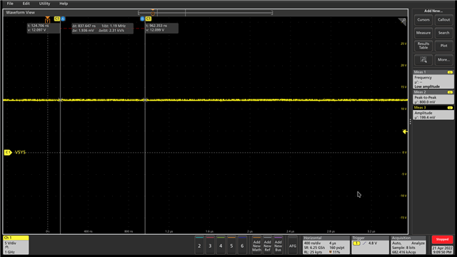
Waveforms

DRVH1: Buck1 High side switch node – high level is going close to 17V.

DRVH2: Buck2 High side switch node

DRVH2_ Cp2: Buck2 High side switch node with repetitive cycles

DRVL2: Buck2 Low side switch node

DRVL2_Cp2: Buck2 Low side switch node with repetitive cycles

Schematic & layout attached for reference. 

pmic_sch, waveform & layout.zip

Please help with your inputs to debug this issue. Thanks in advance for the help and support. 

Regards, S Mathew. 

  • Hi Shinu,

    • What are your power-up sequence settings? Since this is the user-programmable PMIC version I would like to confirm how you have the device programmed (Custom settings or still factory default). If you used the OTP Generator to program the device, a copy of the excel sheet would provide some clarity. Otherwise a full register dump with a short description of the sequence would suffice.

    • Can you provide a scope capture of VSYS, LDO5V0, LDO3P3, and BUCK1? If BUCK1 is not the first regulator to power up just substitute the correct output (this is just my assumption without knowing the power-up sequence). My goal is to follow the power-up process until the first fault is discovered and dissect the issue from there.

    Regards,

    James

  • Hi James,

    Waveforms and OTP details attached.

        PMIC OTP_.xlsx

    Thanks

  • Hi James,

    Once the Buck 2 is enabled , Buck 1 output ripples are there. Without Cntrl 2 enable(Buck 2 enable)Buck 1 output looks fine

  • Hi Srikanth,

    I'm currently looking over the schematic and OTP document, but I have a few questions.

    • Just to confirm, do all rails power up properly with the sequence VSYS > LDO5P0/LDO3P3 > LDOA1/BUCK3 > BUCK4 > BUCK1 > LDOA3 (Without activating BUCK2 yet)? If so, you are seeing GPO1 and GPO2 go high without issue, correct?

    • Is BUCK1 the only other rail affected by BUCK2 enable? Do you observe ripple in any of the other regulators or supply voltages?

    • I see you have over 1.5mF of capacitance at BUCK2 output. Did you use the equations in Section 6.2.1.2.1.2 for your total capacitance value selection?

    I loaded your OTP settings onto our BoosterPack for the TPS65086100 to confirm that the sequence works as expected. I was able to activate all rails without any power faults using the MSP430F5529 LaunchPad development kit and the BOOSTXL-TPS650861. If all the rails connected to CTL1 power up as expected with the sequence I mentioned above, then there may be an issue with the BUCK2 external components if issues only arise once CTL2 is pulled high. Is it possible to test an alternate chip at your location to confirm whether the issue persists or do you only have access to one device?

    Thanks,

    James

  • Hi Srikanth,

    I would recommend removing two of the 330uF capacitors on the BUCK2 output.

    Also I see that R295 on the FBGND2 pin and R297 on the FBVOUT2 pin has been marked DNP. FBGND should have a 0Ohm resistor connecting the line to ground and FBVOUT2 should have a 0Ohm resistor connecting the line to the output node of BUCK2. On BUCK1 you have R288 on the FBVOUT1 pin marked as 0Oms which is different than what is shown on BUCK2 so I want to make sure the FB pins are not floating on BUCK2.

    Try these changes and test the result.

    Thanks,

    James

  • Hi James,

    We had the remote sense populated earlier. Anyway I moved to local sensing by populating those two resistors with 0ohm. But we see that BUCK2 is not turned ON. Highside FET Gate drive is not going beyond 5V. Also we removed 3x330uF, 4X100uF Capacitors from output rail. the behavior remains same on Buck2. It is identified that whatever voltage rails enabled at Stage1(Buck1,Buck3, Buck4) which were stable got disturbed as soon as we enabled CTL2 (enabled for Buck2).

    Buck2 output is like below. Which supposed to be 1V, but we see 0.2V with noise

    Best Regards

    Srikanth

  • Hi James,

    We see that the Buck regulator outputs which were stable earlier in Stage1, got disturbed in the stage2 sequence (by enabling CTL2), The pattern is like below. I just draw the picture of the voltage lines 1.8V, 3.3V . It is strange that oscillatory nature picked up on clean signals. If we measure with multimeter DC voltage shows 1.8V, 3.3V. But oscilloscope showed the below pattern.

    Best Regards

    Srikanth

  • Hi Srikanth,

    Could you provide the layout documentation? If you need to send this information privately I can set up a private message.

    Thanks,

    James

  • Hi James,

    Good news. There is an issue with FET layout symbol. It was not making a contact with Inductor pad due to symbol solder mask was not open to make copper contact. Thanks a lot for your kindly  help till now. I will take your help if I encounter further issue with TI parts.

    BR/Srikanth

  • Hi Srikanth,

    Thanks for using E2E and I'm glad you found a solution! If anything comes up we're happy to help.

    Regards,

    James