Hello,
I was wondering if it's possible to hand solder the TPS82740B given the uSIP package. Do you have any recommendation on how to do it?
thanks
Giorgio
This thread has been locked.
If you have a related question, please click the "Ask a related question" button in the top right corner. The newly created question will be automatically linked to this question.
Hello,
I was wondering if it's possible to hand solder the TPS82740B given the uSIP package. Do you have any recommendation on how to do it?
thanks
Giorgio
Hi Giorgio,
If this is just for assembling a few prototype boards for the purpose of testing, it is no problem. Just make sure to use a lower air speed for the soldering air gun so that the integrated passives don't fly off. Also the TPS82740B should not exceed it's maximum reflow temperature of 260C. Maybe section 5 in this article (snva853b) is helpful.
Best regards,
Varun
thank you for the answer. Yes, it would be just for 1 prototype. I have a couple of additional questions mainly because I've never used the uSIP package:
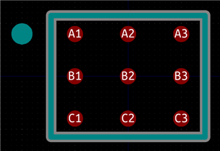
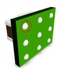
- how can you make sure that the LGA balls a positioned exactly on the footprint pads? the issue is that you can't really see the balls underneath the component. The only way I can see is to make sure that the edges of the component are aligned with the rectangle of the footprint.

- are the balls made of solder and they melt with high temperature? If they don't, then there'll be a gap between the PCB and the bottom part of the component, right?

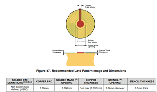
- I found in the datasheet that it is recommended to leave a clearance between the copper pad and the soldering mask. Could you please explain me why? that's not very clear to me.

Hi Giorgio,
It is enough if you align the edges of the component with the rectangle from the silkscreen as best as possible. Once the solder balls of the uSIP melt, they will self align with the closest copper pad.
For proper soldering you need to make sure all the solder balls of the uSIP have melted and made proper contact with the copper pads on the PCB.
It is recommended to keep a small clearance between the copper pad and the solder mask to account for expansion of the solder mask. In case the solder mask expands it can cover the copper pads and reduce contact area for soldering.
Best regards,
Varun