This thread has been locked.

If you have a related question, please click the "Ask a related question" button in the top right corner. The newly created question will be automatically linked to this question.

LM76005: Design help - Vout=5Vx5A - Vin=10~40V

Part Number: LM76005
Other Parts Discussed in Thread: SN65HVD1781, TPS2491, CSD19537Q3, TPS62091, LMR16030, ,

Hi.
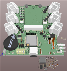
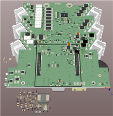
We are developing a board layout which already has these parts from TI:
1x SN65HVD1781
2x TPS2491
2x transistor CSD19537Q3

The board will be supplied by industrial power supplies, 24V nominal. Before, the buck converter was a LMR16030 with 3.3V output, but I changed it by a LM76005 because we will try to add compatibility with Raspberry Pi Compute Module 3 and 4 to it, so I needed to change the main power supply output to 5V using LM76005, because it has more output current capacity, then I'm going to reduce that 5V to 3V3 by using a TPS62091. I need 5V and 3V3 in my circuit.

Please, could I receive an analysis from TI engineers in my schematics and calculations?

SCH-01.pdf


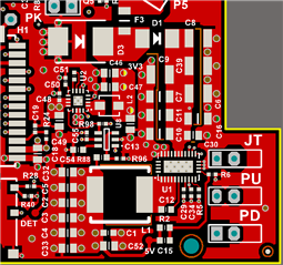
(1) About the TPS62091, here is the Webench design, the inductor I chose is exactly the one suggested on the Webench design.

3513.WBDesign24.pdf


(2) Here are the calculations I did for LM76005 (5V output) until now. OBS: The fact is that in practice, this 5V output will never reach 4A average current consumption.

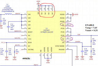
LM76005, Vout of 5V x 5A, Vin of 10 to 40V, 400KHz


------------------------------------
FEEDBACK RESISTORS
------------------------------------
Vin = 10~40V
Vout = 5V
Iout = 5A
Vfb = 1.006V
Resistors = 100K/24.9K
Vout Typ = 1.006+1.006*(100/24.9) = 5.04V
Vout Max = 1.017+1.017*((100*1.01)/(24.9*0.99)) = 5.18V
Vout Min = 0.987+0.987*((100*0.99)/(24.9*1.01)) = 4.87V
------------------------------------
SOFT-START CAPACITOR
------------------------------------
Pin SS/TRK left floating.
Leave this pin floating to use the 6.3ms internal soft-start ramp
------------------------------------
UVLO/ENABLE
------------------------------------
Connections: VIN - RenT - ENABLE - RenB - GND
RenB = (VEN_VOUT_H * RenT) / (VIN_ON_H - VEN_VOUT_H)
VEN_VOUT_H Typ = 1.204V
VIN_ON_H = 9.2V
RenT = 100K 0603 1%
RenB = (1.204 * (100)) / (9.2 - 1.204)
RenB = 15.05K
RenB = 15K 0402 1%
VIN-UVLO-RISING = VENH * (RENB + RENT) / RENB
VIN-UVLO-RISING = 1.204 * (15 + 100) / 15
VIN-UVLO-RISING = 9.23V
VIN-UVLO-FALLING = VENL × (RENB + RENT) / RENB
VIN-UVLO-FALLING = 0.99 * (15 + 100) / 15
VIN-UVLO-FALLING = 7.6V

------------------------------------
SWITCHING FREQUENCY
------------------------------------
RT pin. If floating, the default switching frequency is 400 kHz.
Place a resistor in the layout but do not mount it, at RT pin.

------------------------------------
DUTY
------------------------------------
Dmin = tON-min * fsw
Dmin = (70*10^-9) * (400*10^3)
Dmin = 0.028 (2.8%)
Dmax = 1 - (tOFF-min * fsw)
Dmax = 1 - ( (100*10^-9) * (400*10^3) )
Dmax = 0.96 (96%)
Vin Max and Vin Min.
The maximum operational supply voltage can be found by:
VinMax = Vout / (fsw * tON-min)
VinMax = 5 / ( (400*10^3) * (70*10^-9) )
VinMax = 178V
The minimum VIN without frequency foldback can be approximated by:
VinMin = Vout / (fsw * tOFF-min)
VinMin = 5 / ( (400*10^3) * (100*10^-9) )
VinMin = 125V

------------------------------------
INDUCTOR SELECTION EQUATIONS
------------------------------------
deltaIL = ( (Vin - Vout) * D ) / (L * fsw)
L >= ( (Vin-Vout) * D ) / (0.4 * fsw * I-load-max)
L<= ( (Vin-Vout) * D ) / (0.2 * fsw * I-load-max)
Inductor saturation-current rating.
ILpeak = I-load-max + (deltaIL / 2)
D ~= Vout / Vin

------------------------------------
INDUCTOR SELECTION CALCULATIONS
------------------------------------
Vin = 40V
Vout = 5V
D ~= 5/40
L >= ( (Vin-Vout) * D ) / (0.4 * fsw * I-load-max)
L >= ( (40-5) * 5/40 ) / (0.4 * (400*10^-3) * 5)
L >= 5.46uH
L<= ( (40-5) * 5/40 ) / (0.2 * (400*10^-3) * 5)
L<= 10.93uH
L range = 5.46uH to 10.93uH
* On the tag of the product will be specified a voltage supply range from 12V to 38V.
* On great majority of the cases the supply input will be 24V, from a industrial power supply.
* In history, we have seen only few industrial power supplies, of old machinery, delivering 36V at the maximum.
* Chosen inductor = IHLP3232DZER6R8M11 (Vishay):
- 6.8uH +- 20% (6.8uH * 0.8 = 5.44uH)
- Irating = 7A, Isat = 6.7A
- DCR = 33.4mOhm max
deltaIL = ( (Vin - Vout) * D ) / (L * fsw)
deltaIL = ( (40 - 5) * 0.125 ) / ( (6.8*10^-6) * (400*10^3) )
deltaIL = 1.6A
ILpeak = I-load-max + (deltaIL / 2)
ILpeak = 5 + (1.6 / 2)
ILpeak = 5.8A

------------------------------------
FEEDFORWARD CAPACITOR
------------------------------------
FX = 15.46 / (Vout * Cout)
FX = 15.46 / ( 5 * 6 * (47*10^-6) )
FX = 10.964 KHz
CFF = ( 1 / (2*pi*FX) ) * ( 1 / ( sqrt ( RFBT * (RFBT // RFBB ) ) ) )
CFF = ( 1 / (2*pi*FX) ) * ( 1 / sqrt ( RFBT * (RFBT * RFBB / (RFBT + RFBB) ) ) )
CFF = ( 1 / (2*pi*10.964*10^3) ) * ( 1 / sqrt ( 100000 * (100000 * 24900 / (100000 + 24900) ) ) )
CFF = 3.25 * 10^-10
CFF = 325pF
CFF = 330pF


For the current 6.8uH inductor, I don't wanted to use a bigger physical size inductor (with bigger area), because space is so much 'at a premium'.

Suggestions and recommendations from TI engineers?


Regards.

  • Hi Jefferson,

    Not the LM76005 high-side peak current limit levels, 6Amin, 6.8A typ and 7.8A max.

    Thats basically the maximum peak inductor current before current limit of the SW node comes into effect.

    The safest decision is to have inductors saturation current above the 7.8A max peak current. 

    Those IHLP inductors have soft-saturation characteristics so it should be fine to use those, 

    Just be sure if you change the inductor that the inductance doesn't hard saturate below the max peak current.

    No problem on the 6.8uH, actually you calculated 40% ripple at VIN max when we recommend 20-40% at VIN typical.

    I recommend that 6.8uH value if it works with you.

    If you used 24VIN and 35% ripple current you might be able to use 5.6uH; except 5.6uH will give ~2A pk-pk at 40VIN, so the peak will be ~6A, very close to the minimum peak current limit, so if you need the full 5A at high VIN then I would not use the 5.6uH, especially since inductance decreases with DC load.

    Your output capacitors are likely derated ~20% at VOUT DC bias, you can likely reduce the feedforward to 220pF.

    Everything else on the LM76005 looks good to me.

    Please start a separate thread for that TPS device.

    Thanks,

    -Orlando

  • Hi Orlando, thank you so much!

    (1) I did some research for inductors at Digikey website and I'm going to change the inductor by a ETQ-P4M6R8KVK from Panasonic, they have almost the same RMS current rating, around ~7A (0.1A difference). The saturation current of the previous inductor, the one from Vishay, was 6.7A, but that one from Panasonic the saturation current is 11A. The inductor of Panasonic is a little smaller in area, and they have the same height, 4mm.

    IHLP3232DZER6R8M11 (Vishay) DCR = 33.4mR Max
    ETQ-P4M6R8KVK (Panasonic) DCR = 25.85mR Max
    25.85/33.4 = 0.77

    www.digikey.com/.../6134793

    Do you have something to say about this change?


    (2) About the feedforward capacitor. Ok, I will start with 220pF. And I will try to use 0603 package for it, to be easier to change the capacitor value by hands, if needed.


    (3) About the TPS62091. Ok, I will open another topic.

    Regards.

  • Hi Jefferson,

    The Panasonic inductor is good yes. The lower DCR will have better efficiency and no problem on the saturation current.

    No problem on the 0603 package.

    -Orlando

  • Hi Orlando.

    Here is my updated schematic.

    2185.SCH-02.pdf

    Here is the layout.

    Red color is Top Layer, the board will be 8-layer, the internal layer right below the Top Layer is a ground plane, there is also a 5V power plane, and there will be a 3.3V power plane also, but maybe the 3V3 and 5V rails will share a divided plane, I don't know yet. On previous post I had 6x 10uF 10V ceramic capacitors right at the output, right after the inductor, and then you have suggested a 220pF feedforward capacitor (C15). Now, I have 7x 10uF 10V, right after the inductor, right at the output. You can see that there is an 8th 10uF 10V capacitor at the 5V rail, but it is not placed right after the inductor/output, this 8th capacitor is the C49, it is placed instead very close to the input of the 3V3 buck converter. Considering my new schematic and layout, please, will you recommend another different value for the feedforward capacitor? different from 220pF, as initial value for prototype?

    Regards. 

  • Jeferson,

    Let me review this and get back to you later today.

  • Jeferson,

    Your layout is good. I suggest you tie your DAP to GND and connect to the min top layer GND polygon pour, this will pull heat from the IC and keep it from getting too hot. See the datasheet layout example, or the LM76005QEVM layout images. https://www.ti.com/lit/ug/snvu694a/snvu694a.pdf

    I think in your original calculations you had 47uF caps, I just recalculated with assuming the DC derating. You can look up the capacitor datasheet to get a more accurate DC derating.

    Assuming 25% derating on 80uF total capacitance using equation 22, you'd get ~51kHz Fx. Following equation 23 you'd get around ~69pF so you can probably use 68 or 100pF just fine.

    Hope this helps,

    -Orlando

  • You can also tie some of the NC pins to GND as shown in the layout example and on the EVM.

    -Orlando

  • Hi Orlando.

    I got this result, considering that the 47uF capacitors of output will have only 25% of 47uF due to the DC bias effect.

    ------------------------------------
    FEEDFORWARD CAPACITOR
    ------------------------------------

    47uF * 7 * 0.25 = 82uF

    FX = 15.46 / (Vout * Cout)
    FX = 15.46 / ( 5 * (82*10^-6) )
    FX = 37.7 KHz

    CFF = ( 1 / (2*pi*FX) ) * ( 1 / ( sqrt ( RFBT * (RFBT // RFBB ) ) ) )
    CFF = ( 1 / (2*pi*FX) ) * ( 1 / sqrt ( RFBT * (RFBT * RFBB / (RFBT + RFBB) ) ) )
    CFF = ( 1 / (2*pi*37.7*10^3) ) * ( 1 / sqrt ( 100000 * (100000 * 24900 / (100000 + 24900) ) ) )
    CFF = 9.45 * 10^-11
    CFF = 94pF
    CFF = 100pF (match your recommendation)

    So in the first prototypes we will use 100pF for the feedforward capacitor.

    Regards.

  • Hello Orlando.

    I saw the layout with the ground pour in the document of the link you sent. I understood.

    Please check below:

    (1) Pins 27, 28, 29 and 30 I will connect to GND and make a ground pour to increase heat dissipation.

    (2) Look at pins 19 and 23 above, in purple color. Can I connect these pins to PVIN? In order I can make the polygon of input voltage wider, please check below, is this not recommended?

    Regards.

  • Hi Orlando.

    Please check. I also connected pin 7 (NC) to GND.

  • Hi Jeferson,

    I would keep the pins 19 and 23 floating, I think those are NC to keep a clearance and creepage for VIN when it's high voltage node.

    Same for bootstrap voltage, it swings up to SW+VCC (~VIN+VCC (minus some drops)), so I would also leave pin 7 floating. Pin 7 to GND is not really doing anything for heat either.

    Everything else looks ok to me!

    Hope this helps,

    -Orlando

  • Just to finish.
    This is the 'final' overall layout.
    TPS62091 revised by Varun John.
    LM76005 revised by Orlando Murray.
    I liked the result.
    Thanks very much.
    Regards.