This thread has been locked.

If you have a related question, please click the "Ask a related question" button in the top right corner. The newly created question will be automatically linked to this question.

UCC2808A-2: When we use UCC2808A-2 as the half-bridge circuit topology, the problem of CS pins not working properly/not working

Part Number: UCC2808A-2
Other Parts Discussed in Thread: LM5109, UCC28085, UCC28083

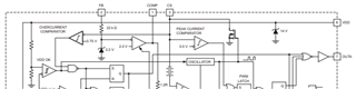
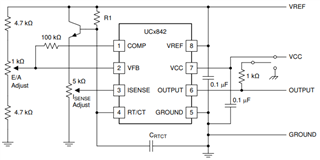
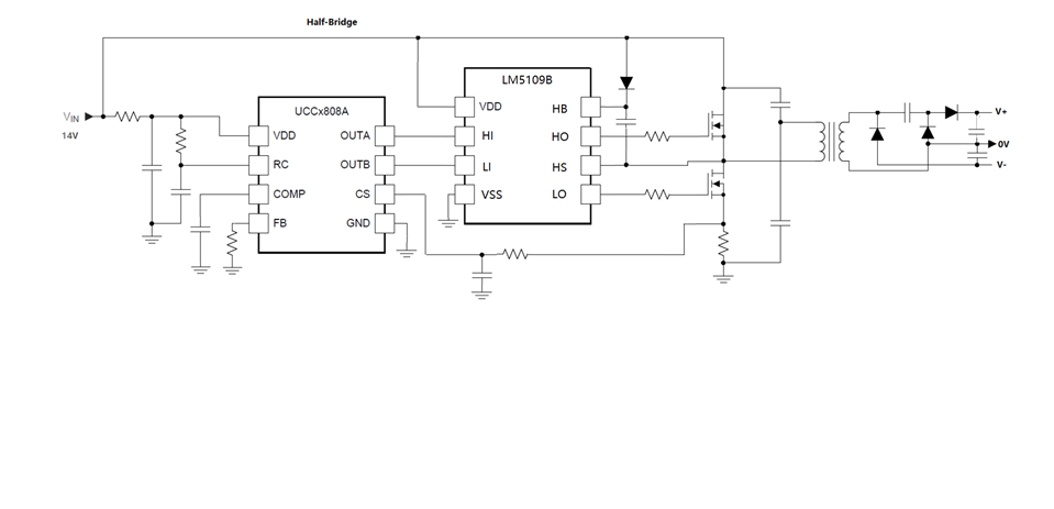
The half-bridge topology we use is shown in the following figure:

We have following questions:
question1:The recommended supply voltage of LM5109BMA given in the datasheet is 14V,but the rated  supply voltage is 18V,leaving 4V as a safety margin,can we use 15V to power the LM5109BMA?

question2:The UCC2808A-2 datasheet gives the threshold voltage of the CS is 0.8V, but we have given the CS voltage more than 2V ,

the CS  cannot turn off the UCC2808A-2.Why and what should we do ?

  • Hello ??,

    1) As you pointed out, the ABS MAX is 18V.  So, the LM5109 should be OK with VDD pin at 15V.  Will there be possibility of transient overshoot on VDD?  Ideally, you should implement an external NPN/Zener based pre-regulator to bring VDD below 14V.

    2) Exactly what do you mean by "the CS cannot turn off the UCC2808A-2"?  When CS > 0.5V the gate drive outputs are turned off.  When CS > 0.8V the UCC2808 will begin a new soft start.  The UCC2808A will never totally turn off, it will change operating modes.

    Pulse-by-pulse current limit is at 0.5V.

    Over current threshold is at 0.75V.

    Block diagram.  Notice the comparators monitoring the CS voltage with 0.5V and 0.75V thresholds.

    I hope this clarifies the operation.

    Regards,

    Eric

  • HI,Eric!

        Thank you for your replies!

        Now, We have another questions and please help us.

       Question 1: As you said "When CS > 0.5V the gate drive outputs are turned off.  When CS > 0.8V the UCC2808 will begin a new soft start."Therefore, we monitored  the CS voltage at 0.5V and 0.8V respectively,You can view the details in the following images.Why and how should we do?

     Question 2: Because of the shortage of materials, we found another IC- ucc28085/3.When we configure the external circuit according to the formula given in the datasheet, we want its frequency to reach 100kHz, so we choose RT=360K,but in fact it is only 50KHz, Why is this?The formula given in the datasheet is as follows.


    Looking forward to your reply!

    Regards,

    XU.LEE

  • Hi Xu,

    1) I see now.  The FB pin is grounded, so the COMP pin is always at it's maximum voltage.  Here is a test circuit from a different regulator that may be useful.  Replace the NPN and 5k-pot with your CS connection (at ISENSE).  Vary the 1k/multi-turn potentiometer to set the duty cycle.  I think something like this will help you see the 0.5V and 0.8V CS threshold functionality.

    2) With RT = 360k the OSCILLATOR frequency is 94.9kHz.  However, it is a push-pull topology so each output switches at half the oscillator frequency.  This is mentioned on page 7 of the datasheet.  It's a little bit before the RT equation.

    Regards,

    Eric

  • Hi  Eric,

          Thanks for your replies again!

          (1)We add a sliding rheostat to the FB pin of UCC2808A-2 for testing according to the method you recommend. We found that when the voltage on FB pin rises to 2.0V, the output pulse of UCC2808A-2 will turn off. This raises another question: at present, our circuit topology is half bridge, and UCC2808A-2 is used in open loop. When the current sense resistance configured for CS pin is enough to meet the normal working needs, can FB pin and CS pin share a network? Our idea is this: when CS and FB share a network and the voltage is below 0.8V, CS works normally and FB does not work because the voltage is not enough. When the voltage exceeds 2.0V, FB starts to work, closes the output pulse and turns off UCC2808A-2.In other words, if we want to turn off ucc2808a-2, how do we configure CS and FB?

         (2)We choose that the resistance at the RT pin of UCC28083/5 is about 160K, and the oscillator frequency is about 105KHz. Is the output of this chip a push-pull topology, resulting in each output switches at half the oscillator frequency no matter whether the external circuit topology is push-pull or half bridge?

    Looking forward to your reply!

    Regards,

    XU.LEE

  • Hi Xu,

    1) The CS pin is for duty-cycle control and current protection.  The FB pin is for regulation.  I would not recommend connecting them.

    1.1) Something just occurred to me.  When you set the CS pin to 0.5VDC there is a specific duty cycle due to the pulse-by-pulse current limit.  Now, when you set the CS pin to 0.8VDC (to test the over current threshold) the duty cycle is unchanged.  This makes sense because the 0.5V pulse-by-pulse current limit threshold is activated before the 0.8V over current comparator can react.  The controller cannot react to the 0.8VDC at the CS pin.

    The 0.8V over current threshold was implemented to take action (generate a restart) when the transformer is saturated or short circuited.  During normal operating conditions the over current protection will not be operational.  To have the over current function generate a restart the CS pin must be pulled high very quickly.  CS must pass through 0.5V and reach 0.8V very quickly, within the CS to Output Delay (typically 100ns).

    2) The switching frequency will always be 50% of the oscillator frequency.  The switching frequencies of OUT1 and OUT2 are derived by the toggle-flip-flop (T flip-flop) shown in the block diagram.  To obtain 100 kHz switching frequency at OUTA and OUTB you have to set the oscillator frequency to 200 kHz.

    Regards,

    Eric

  • Hello again Xu,

    The UCC28023/28025 regulators offer an ILIM/SD pin.  At 1V it shuts off the FETs.  At 1.4V it will generate a re-start.

    You can see the separate ILIM and SD paths in the block diagram.

    Regards,

    Eric