This thread has been locked.

If you have a related question, please click the "Ask a related question" button in the top right corner. The newly created question will be automatically linked to this question.

LM5122: LM5122

Part Number: LM5122
Other Parts Discussed in Thread: , UCC21225A, LM5170

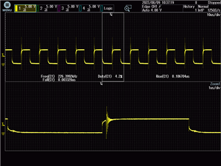
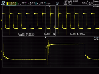
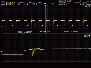
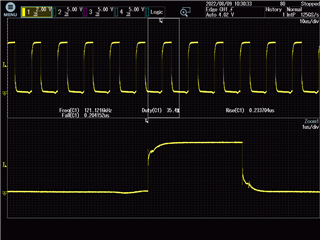
We recently built a two-phase boost circuit using LM5122, with an input of 48V and an output of 96V. However, after each power-on, there will always be a MOS tube that breaks down at the moment of power-on. Where should I investigate this?
mos uses a 200V/100A/11 milliohm, packaged as TO-263;
The circuit design is modified with reference to LM5122EVM-2PH, and the modified circuit switching frequency is 100kHz.

  • Hello xh hxh,

    Thanks for reaching out to us via e2e.

    You are using much higher voltages than our Evm, so you must have modified more than just the switching frequency.
    Could you please share your schematic, so I can verify if everything looks correct?

    Also, can you please provide more details:
    Mow many FETs have been broken so far?  During how many Power-On events?
    Was it always one  single FET each time you tried to turn on or multiple FETs at once?

    Was it always the same FET or different ones that broke?
    If it were different ones: Has the broken FET been replaced and the others which remained on the board could already have suffered from the previous event?
     
    Which FET(s) in which position of the circuitry exactly failed?

    Please let me know as many details as possible.

    Thanks a lot,
    Harry

  • Hello Harry,
     
    We are very happy to receive your reply, and thank you for your support!
    After the circuit is built, when I turn it on for the first time, due to the incorrect value of the feedback voltage, the output voltage is equal to the input voltage (only a dummy load is connected to the output at this time, and the switching waveform is not measured with an oscilloscope).
    The sampling voltage value was modified for the second time, and the output voltage was output according to the expected value (100V). After disconnecting the input, connect the oscilloscope and plan to test the switching waveform of the switch tube in the circuit (the G pole of the switch tube). At this time, the output voltage is 0.4V, the same input voltage is pulled down to 0.4V, and the switch Q3 is overheated and damaged (when damaged, the device has no obvious trauma, and the tin on the pad is melted due to overheating);
    After replacing the switch tube Q3, and no longer connecting to the oscilloscope, the same output voltage is 0.4V;
    Try to remove the switch Q3 to make the circuit work in single-phase, the controllers U1 and U2 are damaged at the moment of power-on (there is obvious damage), among which U2 is particularly serious, and the 18th, 19th, and 20th pins of U2 are blown;
    Finally, the controller was replaced, and the switch tube that was overheated and damaged at power-on became Q4.
    The attachment is the schematic diagram of this circuit and the specification of the MOS(FET) tube, among which Q1 - Q4 use the MOS(FET) tube of the same specification.
    I'm very sorry to cause you trouble due to the doubts in our use!
    Because I also received a reply email, if I have new doubts in the future, can I get help directly by replying to the email?
  • I'm very sorry, the seat of the damaged switch should be Q1 for the first time, and Q2 for the second time. The damaged switches described in the email above should be Q1 and Q2.

  • Hello xh hxh,

    Thanks for the additional information.

    I will have a look at it and come back to you as soon as possible.
    But it may take until beginning of next week.

    Best regards,
    Harry

  • Hello Harry,

    Thank you so much for your help!

    Yesterday I tried to delete the slave control circuit (remove the slave control chip U1, power MOS transistor Q2, power MOS transistor Q4) to change the dual-phase boost circuit to a single-phase boost circuit.
    After re-powering the test, it can be turned on normally, and the output voltage can also meet the design expectations. However, when the output voltage reaches 100V, after adjusting the load size to make the output current exceed 1.2A, the main control chip will be protected and turned off, making the output voltage equal to the input voltage. (48V), after reducing the output current to below 1.2A, the output voltage returns to 100V;
    Similarly, when the output voltage is adjusted to 60V, the output current can reach 5A, but after increasing the output current, the main control chip will be protected and turned off, making the output voltage equal to the input voltage (48V), and reducing the output current to below 5A , the output voltage returns to 60V;
    In view of the above test, new questions have arisen. I set the circuit according to the recommended parameters given by WEBENCH® POWER DESIGNER. When single-phase work, the current should be able to reach more than 10A, and the circuit will be protected during the above test. What is the mechanism and how should I avoid it?
    When using WEBENCH® POWER DESIGNER for circuit pre-calculation, since the online design tool can only provide single-phase design, the output parameters are set to 100V/15A, the input voltage is 36V-54V, and the typical input value is 48V.

    I'm very sorry to cause you trouble due to the doubts in our use!

    Best regards,
    xh hxh

  • Hello xh hxh,

    I want to apologize that I have kept you waiting.
    In the meantime I have had a look at some LM5122 based high power designs to gain some knowledge how real designs look like.

    One important question upfront:  Which power would you like to get across / which current at which voltage shall ultimately be achieved?

    Going back to a single rail would also have been my first attempt. Thank zou for trying this out.

    Here are a few more thoughts and things to try.

    - First thing to check: Make sure that you are not running into any limitation of your lab supply.

    - In case of the lower voltage higher current you are running into current limitation as the shunt resistors atre too low.
          Please consut the datasheet sector  8.2.2.5 Current Sense Resistor RS  how to calculate those.

    - In case of the high voltage you may run into some overvoltage condition.
          Also, this is pretty vlose to the Abs Max Ratings of the part, so there is only minimal margin left.
          Any uncontrolled spikes (due to the swithching of the FETs) may result in an uncontrolled behavior or even damage our device.
          I would recommend that you place a snubber across the Low side FET, to minimize the spikes.

    - In all the high power designs that I have looked at, the LM5122 was set to FPWM mode (Mode pin connected to VCC).
          This would be something to try out as well.

    - For higher currents you may need to reduce the inductance to maybe 22uH. Please be careful with the saturation current of the inductors.

    - Also, have you ckosen 100 kHz switching frequency for a particular reason?

    - The other designs I could compare with were running between 160 and 250 kHz.
        Smaller power quantyties to transmit per cycle, lower ripple, but maybe also higher conduction losses of the FETs.
        Be careful, if you change the frequency, you will need to re-calculate most of the other components in the system.

    All information in this correspondence and in any related correspondence is provided “AS IS” and “with all faults”, and is subject to TI’s Important Notice (http://www.ti.com/corp/docs/legal/important-notice.shtml).


    Best regards,
    Harry

  • Hello Harry,

    Thank you so much for your help!

    First of all, I still prefer to use two-phase or polyphase circuits to achieve high-power output. In doing so, the current carried by each phase will be smaller and more stable. The reason for verifying the single-phase circuit is because in the process of waiting, I want to verify whether there is any problem with my circuit construction.

    Regarding the front-end input limit, there is no one here. The input 48V power supply is a 3500W power supply. Next, I will try to verify that changing the value of the current sampling resistor to check whether the output current can be increased in a high voltage state; Assuming that in the high voltage state, the overvoltage of the main control chip is misjudged due to the switching peak, which can be eliminated by adding a buffer to the FET, then does this affect the switching speed, and the switching loss caused by it will also be corresponding. Increase. Is it possible for me to increase the capacitance of the input capacitor C104 by increasing the feedback voltage? The reason why the switching frequency is set at 100kHz is that the internal resistance of the FET that can be found at this stage is relatively large, and the input capacitance value is slightly larger. If the switching frequency is set too high, it is worried that the FET cannot switch as expected to achieve the purpose of boosting. After verifying the above strategy, I will try to slowly increase the switching frequency to get the best design effect. Another question is, in the case of the same output power (same voltage and same current), the higher the switching frequency of the main circuit, the lower the inductance of the required inductance, so can I use a higher inductance installation and a higher switch frequency in the circuit? Finally, there is still a doubt that in my previous verifications of the two-phase circuit, the output was always 0, and the FET was overheated and burned out. Could this be due to a problem with my circuit configuration? If there is an abnormality in my circuit construction, can you help guide me so that I can correct the circuit.

    I'm very sorry to cause you trouble due to the doubts in our use!

    Best regards,
    xh hxh

  • Hello xh hxh,

    Sure, going back to a single rail was only meant as a first step for debugging.

    Still my question: Which power would you like to get across / which current at which voltage shall ultimately be achieved on the output side?

    Snubbers from Drain to Source of the FETs should not have too much nfluence on the switching time.

    Maybe you should try out a different FET ?

    >> Is it possible for me to increase the capacitance of the input capacitor C104 by increasing the feedback voltage?
    I can neither find C104, nor do I understand the dependency between input capacitor and feedback voltage.
    Can you please explain?

    When increasing the switching frequency, please keep an eye on the inductor current.
    Connect the inductor via a wire, so that you can use an oscilloscope with current probe.

    For the verification of the dual phase concept, would it be possible to try the second phase separately (e.g. disable the first phase via UVLO setting)?
    You would need to remove the connection of the FB pin and VCC and add (another) feedback divider instead.

    Regards,
    Harry

  • Hello Harry,

    Thank you so much for your help!

    I want to achieve 100V/20A (2000W) output in a bi-phase fashion. The output voltage can be adjusted by the adjustable potentiometer to achieve any change between 80-100V; the output current can be arbitrarily changed from 0-20A according to the change of the load.
    The "Is it possible for me to increase the capacitance of the input capacitor C104 by increasing the feedback voltage?" mentioned in the last exchange refers to the feedback voltage input filter capacitor C4 (the capacity marked on the figure is 104). I am very sorry for the difficulty in understanding due to omissions in my writing here!
    If after subsequent debugging, on the basis of solving the existing problems, due to the problems of the FET itself, such as excessive switching loss and frequency limitation, it is possible to consider replacing FETs with different types and parameters.
    I will wait here to verify the state of the circuit when the second phase alone works.
    But before I verified, a new problem appeared, that is, I was still working in the state of the first phase working alone (that is, removing the second phase controller U2, the second phase FET Q2 Q4 in the circuit), the first phase controller is protected. The HO pin of the first phase controller U1 and the LO pin of the first phase controller U1 are both waveform outputs. Measure that the VCC pin of the first phase controller U1 has a voltage of 7.6V, the UVLO input pin detects a voltage of 1.9V (the VIN input pin voltage is 48V at this time), and the FB feedback pin voltage is always 0.8V (that is, the output is equal to the input at this time. , LM5122 did not work).
    According to the manual, when the voltage of the UVLO pin is greater than 1.2V, the controller LM5122 starts to work, but this is not the case at this time, and the reason is not very understood at this time.
    After the above problem occurred, I once suspected that the main control chip was damaged because a colleague accidentally touched the circuit while working overtime on the weekend, but after replacing the main control chip, the above phenomenon still exists.

    I'm very sorry to cause you trouble due to the doubts in our use!

    Best regards,
    xh hxh

  • Hello xh hxh,

    Now as you explained that you would want to achieve 100V/20A (2000W), I have discussed this concept internally.

    We all agree that it is risky to achieve 100V/5A output with only 105V maximum voltage on the SW pin.
    We also believe that two phases will not be enough, as currents will not always be distributed equally between the phases.

    Therefore we would recommend a four phase design, using LM5170 + UCC21225A (isolated gate driver).
    The LM5170 will allow for an adjustable dead time to adopt for the external gate driver.

    All information in this correspondence and in any related correspondence is provided “AS IS” and “with all faults”, and is subject to TI’s Important Notice (http://www.ti.com/corp/docs/legal/important-notice.shtml).

    Best regards,
    Harry

  • Hello Harry,

    Thank you so much for your help!

    I followed the way we communicated earlier and let the second phase in the circuit work alone to verify that the circuit is OK when the single phase is working.
    Indeed, when the second phase works alone, it can work normally, and the output can reach 100V/7.5A. After the output power is increased further, the boost MOS transistor Q4 is damaged. At present, it is not completely judged that it is due to heat dissipation under high power state. The thermal breakdown of Q4 caused by insufficient (since my circuit is mainly used for the evaluation of circuit functions, the corresponding heat dissipation has not been considered too much, and the heat dissipation of the power MOS is mainly solved by PCB copper coating), or it is caused by the saturation of the boost inductor L2.

    I compared the circuits of the first phase and the second phase, and they are completely the same, but when the first phase is working alone, the main control chip U1 cannot start normally, which should be caused by my PCB wiring (but further confirm).

    Earlier you said that it is not recommended to use LM5122 to build a two-phase circuit to achieve 100V/20A output, which is prone to the phenomenon of insufficient two-phase current sharing.
    But can't our LM5122 realize multi-phase parallel connection? When a multi-phase control chip is used to build a circuit, can the current sharing be understood as adaptively realized by the main control chip?
    Assuming that the LM5122 cannot achieve complete current sharing, I designed the output of the circuit to be 100V/30A in the previous parameter calculation and design, and what I actually used was a power change of 100V/20A (0-20A). Is it possible? ?
    Or I use a single-phase circuit to achieve 100V/15A, is it feasible?

    When I was verifying the work of the single-phase circuit, I had a new question that I wanted to ask, that is, when the output power of the circuit is greater than 3A, the waveform measured by the gate of the FET will have obvious ringing phenomenon (as shown in the attached picture), What kind of extra work do I need to do on the FET driver circuit?

    I'm very sorry to cause you trouble due to the doubts in our use!

    Best regards,
    xh hxh

  • Hello xh hxh,

    I am sorry, my previous post must have been completely misleading and I found a typo in there.

    I meant to say the following things:

    1) It is highly risky do design a system for 100V output, if there is only 5V margin left.
    Any ringing or voltage change caused by a load dump will easily exceed the 105V and will destroy your system sooner or later.
    Therefore, we would recommend using external isolated gate drivers UCC21225A.

    2) The LM5122 is not suitable for external gate drivers because it cannot djust the dead time.
    The LM5170 instead will allow for an adjustable dead time to adopt for the external gate driver timing.

    3)We believe that two phases will not be enough to achieve 100V/20A output power, so we recommend using four phases instead.

    4) The LM5122 has been designed for multi-phase parallel connection.
    It does support the phase shift between the phases, it can handle on common feedback loop and compensation and a synchronized behavior in case of errors.

    Nevertheless there is no active current sharing mechanism between the two controllers.
    Therefore, the current distribution varies with tolerances of the (external) components and it especially depends on the layout of the board, how much current will flow via which path.
    To achieve a (nearly) perfect distribution between the two controllers you would need to add an external amplifier that senses the difference between the two and regulates the slave accordingly.
    In most cases this is not done that way. Instead customers leave some more margin to compensate for the higher current across one phase.

    To reduce ringing on the Gate side, you may want to introduce Gate resistors (maybe with a diode in parallel) and maybe also some small caps between G and S or G and D to slow down the switching of the FET.

    If you also see ringing on the switch node, here are some papers which explain what you can do to reduce that:


    https://www.ti.com/lit/an/slva255/slva255.pdf?ts=1660066058248&ref_url=https%253A%252F%252Fwww.ti.com%252Fsitesearch%252Fen-us%252Fdocs%252Funiversalsearch.tsp%253FlangPref%253Den-US%2526searchTerm%253Dfet%2Bringing%2526nr%253D3507

    https://www.ti.com/lit/an/slvaee3/slvaee3.pdf?ts=1660064208000&ref_url=https%253A%252F%252Fwww.ti.com%252Fsitesearch%252Fen-us%252Fdocs%252Funiversalsearch.tsp%253FlangPref%253Den-US%2526searchTerm%253Dmultiphase%2526nr%253D1325
    https://www.ti.com/lit/an/slvaee6/slvaee6.pdf?ts=1660064214005&ref_url=https%253A%252F%252Fwww.ti.com%252Fsitesearch%252Fen-us%252Fdocs%252Funiversalsearch.tsp%253FlangPref%253Den-US%2526searchTerm%253Dmultiphase%2526nr%253D1325

    Best regards,
    Harry

  • Hello Harry,

    Thank you so much for your help!

    Regarding the suggestion you gave me about the drive circuit, I will correct and verify it on the basis of solving the abnormality in the circuit when the two-phase parallel operation is performed. Thank you so much for your valuable advice and guidance documents.

    Now I see why you recommend me to use a 4 phase circuit. In the early stage of building the two-phase circuit, I considered the current sharing problem you mentioned, so the power output of 100V/20A has a margin in the design of both voltage and current. The actual rated demand of my post-stage load is 95V/13A (80-96V and 0-13A), so based on my actual demand, the two-phase circuit should be able to meet the requirements, right?
    The problem encountered now is that the existing circuit, which performs the independent operation of the second phase on the existing circuit, can output 100V/7.5A under the condition that the input is 48V, but the two phases are operated at the same time or the first phase is independent. When the phase is running, when the input is 48V, the output can only reach 100V/2A. Is this a problem with the construction of my circuit? The circuit is realized by adjusting the parameters according to the reference design LM5122EVM-2PH. Are there any minor modifications to this reference design that are not available on the TI website? Can you tell me about these minor modifications, or help me correct my existing circuit deficiencies or areas that need to be improved.

    I'm very sorry to cause you trouble due to the doubts in our use!

    Best regards,
    xh hxh

    升压板0497.SCH

  • Hello xh hxh,

    In the beginning of that thread you had mentioned that Q1 broke.
    At that time also Q3 and even the LM5122 of the first phase may have got damaged.


    Again, the Abs Max rating is 105V.  When Q1 broke, there may have easily been a spike which was higher than that.
    A stressed / damaged part can look good from the outside it may even work partially but not give you the full performance.

    Can you maybe replace the FETs and the LM5122 from the first phase and start new tests with a low output voltage?

    Thanks and regards,
    Harry

  • Hello xh hxh,

    I have not heard from you for two weeks now, so I assume your problem has been solved and I will close this thread.
    You can re-open it or simply start a new one if this one got locked.

    Best regards,
    Harry