This thread has been locked.

If you have a related question, please click the "Ask a related question" button in the top right corner. The newly created question will be automatically linked to this question.

UCC27282: Bootstrap diode burned out

Part Number: UCC27282
Other Parts Discussed in Thread: CSD19536KCS

Hello team,

I am writing because I am doing in design of an inverter with the UCC27282 and the CSD19536KCS.

 The circuit works fine up to 24Vdc, but, when I try to bring the supply voltage to 50Vdc the bootstrap diode burns out. What could be happening?

 I am attaching the schematic.

Thank you very much.4137.Schematic.pdf

  • Hello Jorge,

    I reviewed your schematic and It looks like the bootstrap capacitor and VDD capacitance values should be OK to support the Mosfet gate charge. Can you provide some details on the design such as switching frequency, minimum and maximum duty cycles of the HI and LI driver inputs. 

    I do have one comment, the Mosfets you are using are relatively low gate charge, and I see the gate resistances are low with 3.3 ohms turn on and 1.2 Ohms turn off. This may result in very high dV/dt on the switch node. This high dV/dt can result in high voltage overshoot and undershoot which can be an issue for the driver.

    Can you provide scope plots of the LO output, HO-HS output, and HS waveform with a time scale showing several cycles, and a zoomed in scale to see the turn on and turn off details? You can do this in the safe operating condition to start.

    Regards,

  • Hello Richard,

    Thank you very much for your reply.

    Some details of the design:

    • Switching frequency: 20KHz.
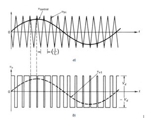
    • Duty cycle: being an inverter, the control of the UCC27282 is by PWMS. So, the duty cycle is variable. But I can give you the amplitude modulation ratio which is ma = 0.9. and the frequency modulation ratio is mf = 50.

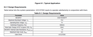
    • Regarding the Rgate value, I just followed the example in the UCC27282 datasheet.

    • In the case of the inverter, I am using the CSD19536KCS.

    • The LO, HO-HS and HS images will be sent to you in these days.

    Finally, I attach a pdf file with the PCB design.

    Regards.

    Some details of the design.pdf2260.PCB.zip

  • Hello Jorge,

    Thank you for the information on the application, I am somewhat familiar with the sin wave modulation method, and 20kHz switching frequency does sound similar to other inverter apps. If you happen to know if there is any minimum pulse width limits which can be applied to the high side driver, or low side driver that will be helpful. The concern of interest, is that the boostrap capacitor needs have the voltage recharged when the switch node switches to ground which is normally when the low side driver is on. If the LO output may have narrow pulses this may lead to the boot capacitor not being fully recharged, when the switch node goes high. This can lead to stress to the diode.

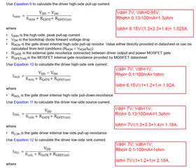
    The driver currents you show from the apps example in the datasheet is not a concern. I know from general testing that the relatively low Qg Mosfets will switch fast with low value gate resistance. This fast switching speed is probably not really needed at 20kHz switching frequency.

    I will look at the board plots, which may take a little time, if you can look into getting some scope plots in the mean time that will be very helpful to resolve your concerns.

    Regards,