This thread has been locked.

If you have a related question, please click the "Ask a related question" button in the top right corner. The newly created question will be automatically linked to this question.

TPS61178: TPS61178

Part Number: TPS61178
Other Parts Discussed in Thread: TPS61288, LM3488, LM3478, LM3481, LM3481-Q1, LM5176, LM34936, LM34936-Q1, LM5118, LM25118, LM5176-Q1, LM25118-Q1, LM5118-Q1

Hi TI Team,

Earlier, We have communicated with TI Team regarding the TPS61178 switcher part and they were given confirmation for TPS61178.

e2e.ti.com/.../4148405

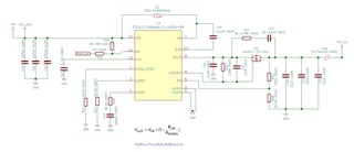
We are giving 3.0V to 4.2V supply to the switcher and we want to generate 12V, 2A from this switcher. I am attaching our circuit diagram for your reference and we have already verified the schematic with TI earlier.

Board is restarted when the current output is >0.5 A.

We have connected resistive load to the switcher output and increased the load slowly and when it is reached at 0.6A, the board is restarted so switcher is giving 12V, 0.6A output only when the input voltage is 3.8V.

So please provide your technical guidance for the same. We want 12V, 1.2A stable output. Board is already designed and our hand.
  • Hello TI Team, 

    Would you please check thread from your end and suggest solution from your end as we have already designed board as per your recommended IC and now we are completely stuck like Switcher is not seems to be working as per reference design. 

    It would be really appreciated if you give feedback as quickly as possible. 

    Regards, 

    Ritesh Prajapati

  • Hello ,

    Would you please check and suggest like what can be the possible reason behind issue of voltage drop out while using TPS61178 IC? We really need your help and support for the same.

    Because we have designed board based on confirmation from your end with design review as per requirements and now it is not working as per expectation and requirements.

    So, Please check thread with details from your end and helps us to find out possible cause with suggestion to resolve it.

    Regards,

    Ritesh Prajapati

  • Hello TI Team,

    Please find attached BOM Report with manufacturing part number for each and every component related to TPS61178 Switcher as per design shared into main thread.

    So, Please check that as well from your end and let us know if any issue or any deviation into any of part which we have selected

    BOM_Report_TPS61178_Switcher.xlsx

    Regards,

    Ritesh Prajapati

  • Hi Ritesh,

    Sorry for reply late.

    Please could you have a test of the waveforms of SW,Vout,VCC12,IL2 at the moment  the voltage drop out OR restart as you mentioned.

    You can use sudden current load >0.6A to trig the waveform as well as the increased the load slowly.

    If there is other abnormal situation, please record the waveforms at the same time.

    Your test result will help to  location the problem.

    I will discuss with Zack to help you together.

    Best Regards,

    Fergus He

  • Thanks for your response with details. We will provide reports with signals as requested. 

    But Meanwhile, would you please check BOM of Switcher Circuit and components as well as Switcher Circuit Design which have been shared earlier? Is there any issue into any component or BOM? Or any issue into Switcher Design Circuit? 

    Regards, 

    Ritesh Prajapati

  • Did you get chance to check BOM of Switcher Circuit and components as well as Switcher Circuit Design which have been shared earlier? Is there any issue into any component or BOM? Or any issue into Switcher Design Circuit? 


    Regards,

    Ritesh Prajapati

  • Hello ,,

    We have captured waveforms as per your requested points and attached complete report with details from our end.

    4300.TPS61178_Report.pdf

    Click here to play this video

    Also, I have attached in 12V, 400mA Output waveforms are being captured. So, you will also more details into PDF Report in which device is also going to shutdown while increasing load at input end.

    So, Would you please review both Report and Video from your end and suggest feedback to move further? Also, I have attached Switcher BOM Reports earlier with each and every component part number. So, Please review that as well like is there any issue into any component or part.

    Also let me know if you are not able to download MOV Video File at your end.

    Regards,

    Ritesh Prajapati

  • Hi Ritesh,

    1. I'm sorry for not able to download MOV Video File.

    2. I found that there's two inductors in the BOM, No.8 and No.9 . And the inductance seems not match that in SCH. Please explain this.

    3.I may not have make it clear that the signal should better to be tested in one picture.

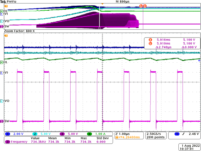
    Please have a detail waveform with the Vin(PIN 12) ,SW(PIN7), inductor current(test with a current probe series with inductor) and VOUT(PIN 8)  in one picture. Two situations are needed, 140mA and 410mA(just as you did).

    As is shown in Fig 7, the waveform can be different when Vout is in peak and trough, please capture different pictures at the two periods. 

    if the waveform is indistinct, please change to smaller time axis so that it can show waveform clearly. 

    see the sample like this.

    We will have a better understanding of your problem.

    Thank you

     Fergus He

  • Hello 

    Thanks for your feedback with comments. 

    We will capture signals again as per your instructions and will send it again with proper format of video file and will share to you ASAP. 

    Regards, 

    Ritesh Prajapati

  • Hello ,

    Please find attached MP4 file which we have converted from MOV file and also shared it over WeTransfer Link if not able to download from here.

    Below is link for Video File over WeTransfer

    https://we.tl/t-Ne44i26B1e

    Let me know if still not able to access it from your end.

    Can we discuss over quick call or separate email thread for quick discussion to get urgent support because we are completely stuck to deliver our product due to this type of issues? Please suggest your best way to discuss it. 

    Regards,

    Ritesh Prajapati

  • 2. I found that there's two inductors in the BOM, No.8 and No.9 . And the inductance seems not match that in SCH. Please explain this.

    Hello ,

    I think there is some misunderstanding into BOM Report view from your end as there is only single Inductor has been used into Switcher Circuit. Please see below screen shot for the same

    Part No - 8 is Ferrite Bead not an inductor.

    Would you please check it again from your end?

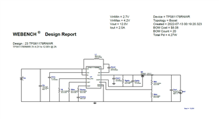
    Also regarding Inductance, We have kept 3.3 uH into Schematic but taken it as 1 uH as per Work Bench Design for TPS61178. 

    Below is Workbench Design for reference.

    Let me know if need anything else from my end as per your query regarding schematic design and BOM Report.

    Regards,

    Ritesh Prajapati

  • Hello ,

    I have checked BOM Report of Switcher with Schematic and there is mistake into BOM Report regarding inductor. So, Please find following correct inductor number which has been used as per schematic

    Inductor Part Number - ETQ-P4M3R3KVK Panasonic

    Let me know if need anything else from my end

    Regards,

    Ritesh Prajapati

  • Please have a detail waveform with the Vin(PIN 12) ,SW(PIN7), inductor current(test with a current probe series with inductor) and VOUT(PIN 8)  in one picture. Two situations are needed, 140mA and 410mA(just as you did).

    As is shown in Fig 7, the waveform can be different when Vout is in peak and trough, please capture different pictures at the two periods. 

    if the waveform is indistinct, please change to smaller time axis so that it can show waveform clearly. 

    Hello ,

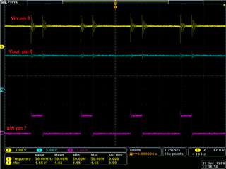
    We are not able to measure signal on inductor current as we don't have equipment to measure it over here but we can able to get Waveforms on Vin, Vout and SW Pins which are below

    We have updated C18-C20 capacitors like We have used 10uF (GRM21BR61E106KA73L) 2x parallel capacitor with Total 20 uF. Also changed R18 to 15KOhm (RMCF0603FT15K0). We have also changed C14 Capacitor to 6.8 nF (CAP-6800pF-50V-0603). R17 also has been changed to 86.6 KOhm.

    Both Attached Waveform signals are with current load as 700 mA.

    Let us know if need anything else from our end.

    Regards,

    Ritesh Prajapati

  • It seems that now you can work normally with current >400mA,

    could you tell me how you get the change of parameters of R18,R17 and C14?

    And now can you work at current of 2A as you designed initially?

    Fergus He

  • Hello ,

    Yes. But when it reaches beyond 700 mA like 710 mA then board is going to shutdown.

    We have received change of parameters of R18, R17 and C14 from Zack Liu.

    So, We are not able to test at 2A load because board is going to shutdown after 700 mA load.

    Let me know if need anything else from my end.

    Regards,

    Ritesh Prajapati

  • At 710mA situation, is the shut down waveform same as the 410mA shutdown waveform before?

    Please have a test of the waveform that just like you did for 700mA situation.

    Thanks,

    Fergus He

  • Hello ,

    Yes. We have checked and quality has been improved into 710 mA load current like we have shared waveforms for 160 mA load in which board was working fine.

    We will share waveforms to you for reference ASAP.

    Regards,

    Ritesh Prajapati

  • Hello ,

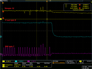
    We have also captured signals over 710 mA when board is going to shutdown and below is image contains Waveforms for Vin, Vout and SW Pin

    Let me know if need anything else from my end.

    Regards,

    Ritesh Prajapati

  • Hi Ritesh,

    Please change the setup of your telescope, your sampling point and the ACQ should as high as possible.

    Now it is 50k/s and 10k points the waveforms are totally distorted.

    And if it is possible, please provide your PCB layout to have a check, you can send mails to me and Zack.

    Fergus

  • Thanks  for providing response. 

    Let me check your queries regarding setup requirements with my hardware team and will get back to you if any queries from our end. 

    Also would you please send an email of Jack as well so will send Layout Design to both of you as per your request? 

    Regards, 

    Ritesh Prajapati

  • Hello  @Zack Liu,

    I have shared Layout Design into personal message to both of you.

    So, Please check it from your end and let us know feedback for the same.

    Regards,

    Ritesh Prajapati

  • Hi Ritesh,

    I've discussed with Zack, and he has given you advice for layout.

    Please provide the test waveform we mentioned before, that will help to find out if there is other design problem.

    Thanks

    Fergus

  • Thanks for providing response and also thanks for Zack as well.

    We will test waveform as per your request and will provide results from our end.

    Regards,

    Ritesh Prajapati

  • Hello  and 

    Would you please check below conversation which is similar to us like he mentioned not getting proper output and getting too much noise while using TPS61178 ans TPS61288 both? 

    e2e.ti.com/.../tps61178-part-not-working-properly

    We just want to know that issue has been resolved ot not? If resolved then solution is from hardware side or not?

  • Hello  and 

    Based on last response with link I have mentioned, We had couple of queries regarding issue which we are facing and few scenarios mentioned into that thread of TPS61178 not working thread

    1. You have suggested one new compensation network Rc =  3 Kohm and Cc = 10 nF. Based on which ESR of our output capacitor these values have been derived because we are unable to find ESR value of Cout Capacitors (P/N# ) from the datasheet.

    2. Few Murata Series Caps shown ESR value vs Frequency. so which value we need to consider for ESR for Rc and Cc calculation to design Compensation network.

    3. Can you please describe in detail how compensation values have been calculated in datasheet section "9.2.4.4.2 Loop Compensation Design Steps" ?

    4. what are the parameters we need to consider for

    5. what values we need to consider for

      1. KEA is gain of the error amplifier network
        • KPS is the gain of the power stage

  • Hello  and 

    Would you please provide us reference Gerber of EVM Gerber to compare with our layout?

    Regards, 

    Ritesh Prajapati

  • Hi Ritesh,

    Zack has provide Gerber of EVM to you, please connect us if you have any questions about the EVM board.

    Best Regards

    Fergus

  • Hello 

    Yes. We have received Gerber files from Zack but Zack has told that now we need to contact to you for further assistant regarding this issue. 

    We would also like to know that can we achieve Output as 12 V 2 A having input voltage as 3.3 V to 4.2 V Battery Voltage with 7800 mA Battery using TPS61178 EVK provided? 

  • Hi Ritesh,

    You can use TPS61178 EVM board for 3.3V- 4.2V input and 12V 2A output.

    Please be careful the default output voltage of EVM board is 16V, you should change the feedback resistor(R1 and R2) to adjust the output voltage to 12V.(R1 change to 732k and R2 remains 80.6k)

    Please refer to the EVM User's Guide.

    EVM User's Guide.pdf

    Best Regards

    Fergus

  • Hello 

    Sorry but we have checked into User Guide and Datasheet of EVM in which we can't get much output voltage like 12 V 2 A as per table mentioned. I will provide that table tomorrow with some details ss well. 

    Regards, 

    Ritesh Prajapati

  • Hello ,

    Sorry but here you have mentioned that it will give 16V Output but you haven't mentioned current as well. Because we have checked into EVM Datasheet or Specifications and found below details in which we can't able to get 12V 2A constant load as per our requirements

    Because Input Voltage is 3.3V to 4.2 V 7800 mA Battery Pack supply and i don;t think with that much of input power we are able to get output power of 12V 2A as per above table.

    Please confirm from your end as well.

    Regards,

    Ritesh Prajapati

  • Hello ,

    Would you please provide settings of below to meet our requirements 3.3V to 4.2V 7800 mA  and output 12V 2A constant load?

    1.2 Modification
    The external components of the TPS61178 device can be modified to adjust the output voltage, input
    current limit, switching frequency, and response speed for real applications.

    Would you please provide modifications as mentioned into datasheet section 1.2?

    Regards,

    Ritesh Prajapati

  • Hi Ritesh,

    To change the output voltage to 12V, you just need to change R1 to 732K

    I have verified this on my EVM board, it can output 12V 2A with 3.3v-4.2vin

    If you have any other questions, please tell me.

    Regards,

    Fergus

  • Thanks  for providing prompt response.

    I would like to know that how you have verified output 12V 2A? Means through resistive load or inductive load?

    Regards,

    Ritesh Prajapati

  • Hi Ritesh,

    It is constant current load 2A, use Electronic load.

    Regards,

    Fergus

  • Thanks for providing required details.

    I will let you know if any further query for the same.

    Regards,

    Ritesh Prajapati

  • Hello ,

    As we are still into discussion regarding TPS61178 issue and It will take still time to get actual issue resolution.

    In parallel, Would you please suggest us any other alternative which can fulfil our requirements or any other suggestions from your end? So that we can also evaluate that into parallel as per our requirements.

    Regards,

    Ritesh Prajapati

  • Hi Ritesh,

    1. For your issue, we still look forward to analysis your failed waveforms.

    Please refer to former tips like choose appropriate sampling point and ACQ.

    2. You can use TI tools to have an alternative solution in website,

    Step-up (boost) regulators product selection | TI.com

    after choose the chip ,you can use Webench to get schematic and BOM guidance.

    Regards

    Fergus

  • Thanks for your prompt response.

    But, We are not able to move further with TPS61178 as we did all types of testing from our end. Let me know from your end like what kind of details are still required from your end to move further.

    In Parallel, We are also planning to send few queries with requested waveforms from our end.

    Regards,

    Ritesh Prajapati

  • Hello ,

    I have checked Step-Up Boost Link which you have provided

    But, I am still not able to understand that it shows 15A or < 15 A Switching Current while into our case we need 12V 2A Constant Load as Inductive Load to operate Heater which is supporting maximum 12V 4.2A.

    So, We are completely confused with the specification given and to fulfil our requirements.

    Can you please suggest at-least 2 to 3 parts which can fulfil our requirements for input 3V to 4.2 A having 7800 mA and output 12V 2A constant load with inductive load?

    Regards,

    Ritesh Prajapati

  • Hi Ritesh,

    It's just like we discussed before.

    Please have a detail waveform with the Vin(PIN 12) ,SW(PIN7),  and VOUT(PIN 8)  in one picture.

    Use the Vout drop to trig the waveform (single mode is recommended) and choose appropriate time axis, sampling point and ACQ to make sure we can see every SW waveform clearly(like the picture I attached before).

    If you are still confused how to capture , please raise your detail questions about the testing.

    Thanks 

    Fergus

  • Thanks ,

    We will send requested Waveform with queries from our end. Would you please send response of second query which I have asked earlier?

    I have checked Step-Up Boost Link which you have provided

    But, I am still not able to understand that it shows 15A or < 15 A Switching Current while into our case we need 12V 2A Constant Load as Inductive Load to operate Heater which is supporting maximum 12V 4.2A.

    So, We are completely confused with the specification given and to fulfil our requirements.

    Can you please suggest at-least 2 to 3 parts which can fulfil our requirements for input 3V to 4.2 A having 7800 mA and output 12V 2A constant load with inductive load?

    Regards,

    Ritesh Prajapati

  • Hi Ritesh,

    You can find the 3 designs here:

    Power Designer (ti.com)

    Power Designer (ti.com)

    If you want to use controller (external switch),there will be more choice.

    Thanks 

    Fergus

  • Hi Ritesh,

    I have questions about the constant load with inductive load you mentioned,

    Can you explain it for me? It is not a just a resistor of a inductor?

    How its current changes with its voltage?

    Thanks

    Fergus

  • Hi Ritesh,

    You can find the 3 designs here:

    Power Designer (ti.com)

    Power Designer (ti.com)

    If you want to use controller (external switch),there will be more choice.

    Thanks 

    Fergus

    Hello,

    But, Here Output Voltage is 3.3V while we need output voltage as 12V with 2A constant load.

    Regards,

    Ritesh Prajapati

  • Hi Ritesh,

    I have questions about the constant load with inductive load you mentioned,

    Can you explain it for me? It is not a just a resistor of a inductor?

    How its current changes with its voltage?

    Thanks

    Fergus

    Hello,

    I thin you misunderstood my output load with requirements. Let me explain it again.

    We are connecting our Main Board with Heater which consumes 12V Constant with variable output current from 0A to 2A based on Heater requirements. So, When Heater needs more current at that time it will consumes more current from Switcher.

    So, There is constant 12V Output but Output current will be varied based on Heater requirements and in some cases it will also consumes constant load of 12V 2A based on Heater requirements.

    Let me know if still you have any queries for the same.

    Regards,

    Ritesh Prajapati

  • Hi Ritesh,

    Understood.

    You means the output ranges from 0A to 2A.

    Thanks

    Fergus 

  • Hi Ritesh,

    You can find the 3 designs here:

    Power Designer (ti.com)

    Power Designer (ti.com)

    If you want to use controller (external switch),there will be more choice.

    Thanks 

    Fergus

    Hello,

    But, Here Output Voltage is 3.3V while we need output voltage as 12V with 2A constant load.

    Regards,

    Ritesh Prajapati

    Hi Ritesh,

    Sorry for the wrong link.

    try this Power Designer (ti.com), type the input and output then click UPDATE DESIGNS

    it will show all the reference designs, you can choose converter(integrated switch)  or controller (external switch).

    Click any design to see details.

    Best Regards

    Fergus

  • Yes. Exactly. Output is from 0 A to 2 A load based on output load requirements. 

    Let me know if need anything else from my end regarding input and output requirements. 

    Regards, 

    Ritesh Prajapati

  • Thanks for providing link. 

    Let us evaluate it from our end and will let you know if any further query for the same. 

    Regards, 

    Ritesh Prajapati