
- Ask a related questionWhat is a related question?A related question is a question created from another question. When the related question is created, it will be automatically linked to the original question.
Hi Power Team,
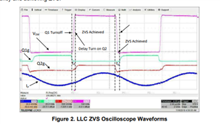
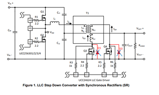
I'm confused about figure 2 in application report SLUA923. Figure 1 shows upper Mosfet as Q1 and lower as Q2. Figure 2 and other places throughout the report show Vsw node low when Q1 gate is high. Shows Vsw node at V+ when Q2 gate is high.
I believe the notations for Q1g and Q2g are swapped.
Regards,
Stuart


