This thread has been locked.

If you have a related question, please click the "Ask a related question" button in the top right corner. The newly created question will be automatically linked to this question.

UCC27211A: What's the behavior when LI pin is permanently high?

Part Number: UCC27211A
Other Parts Discussed in Thread: UCC27211

Hi, Team

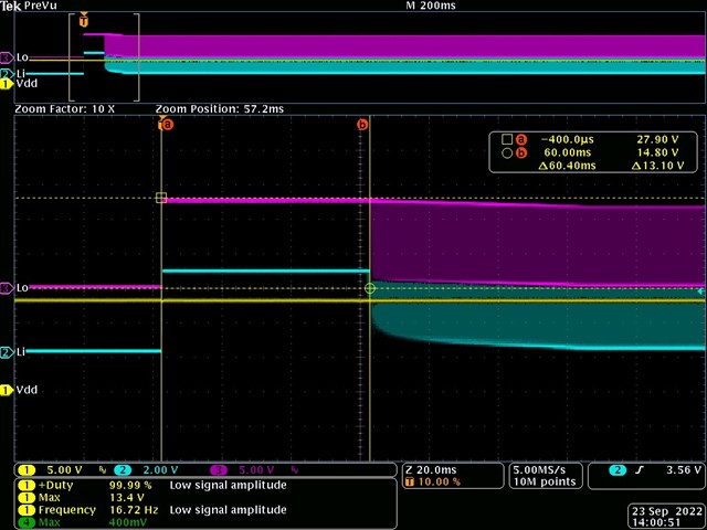
Our customer use our UCC27211A in their BBU project, our device work's well in normal condition. 

But when they try to permanently Pull Li pin as high , they found that the LO pin will become low.

Does our device have any protection feature to make sure Lo pin will not permanently pull high?

Could u help to give some suggestions?

Thanks.

G.W

  • Hello GW,

    There is not any specific protection feature in the UCC27211 that should limit the LO being high when LI is high. Can you confirm the pin signals on the IC including LI, LO and VDD to confirm that VDD is stable, and above UVLO during the behavior you mention? If you can attach scope plots that will help determine the issue.

    Regards,

  • Hi, Richard

    Pls check the waveform, thanks.

    UCC27211A issue.pptx

  • Hello GW,

    Thanks your for the waveforms and information. I am reaching out to investigate this issue. I do see that the input is rising at the same time that VDD is not above UVLO and stable. Is there a way to test with LI rising delayed until VDD is above UVLO and stable?

    Regards,

  • Hi, Richard

    Pls check the waveform.

    as you can see, the waveform return correct when we apply the VDD first. See below picture for your ref.

    So it seems the issue is relate to the power sequence.

    And customer prefer to check below question to us:

    1, If we apply the VDD and Li at the same time, why our Lo output can't follow the Li?

    2, When the issue happens, the Lo output can return to normal while PWM input to Li. Why? It seems the rising/falling edge can recover the  Lo to normal?

    Customer is used in BBU project for server system, so the reliability is very importance. 

    They worry about there is any other risk on our device. So they needs the mechanism about the issue.

    Thanks.

    G.W

  • Hello GW,

    Thank you for confirming the operation with VDD applied 1st before LI. At this time I am not sure of the exact cause of the behavior with LI and VDD rising at the same time. At this time I am not in the office until next week, I will have to investigate when I am back in the office next week. My suspicion is this is related to the UVLO delays  not ready and the impact on the driver level shifter circuits. But this does need to be confirmed.

    Regards,

  • Hi, Richard

    Do u have any new finding about this case? Customer is waiting for our feedback.

    Thanks your help.

    G.W

  • Hello GW,

    I have not had a chance to determine exact root cause. I would recommend applying VDD 1st before the application of the PWM signals since there is a UVLO delay. Is this sequence acceptable for the customer, as it is recommended so that you can predict the LO behavior timing since there is a UVLO delay of several us.

    Regards,