This thread has been locked.

If you have a related question, please click the "Ask a related question" button in the top right corner. The newly created question will be automatically linked to this question.

TPS61175 current efficiency

Other Parts Discussed in Thread: TPS61175, TPS40210, TPS62111

Hi,

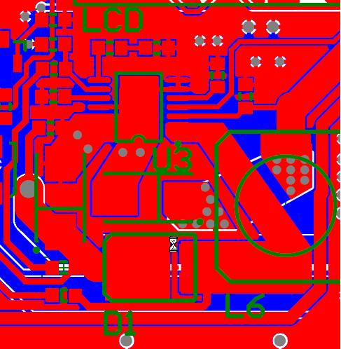
I used TPS61175 for step-up regulator. It should works with parameters as follows: Vin: 4V...7V, Vout= 11.5V, output current up to 1.5A. Coil presented on the schematic is MSS1038 - 15uH. Configured output voltage is Ok, but achieved efficiency is much less than expected. What is wrong and what should I do?

Regards,

Kamil

3056.Schematic.pdf

  • Per equation 6 in the datasheet, the TPS61175 cannot be guaranteed to provide your output power needs.  That is, when using the minimum guaranteed value of current limit (3A), the IC may current limit if you try to demand 10.5V at 1.5A from a 4V source.  You can either respec your power needs, move to the TPS40210 controller, or split up your 10.5V rail into 2 or more pieces.

    As to efficiency, what efficiency were you expecting, where did you get these expectations, and what efficiency are you measuring?  Make sure to measure Vin and Vout right at the IC to not factor in any losses in the PCB traces.


  • I've noticed your tips, and I tried following steps:

    1) I connected 6VDC to the TPS61175 and I supposed at least 1.2 A output current. Using constant load (13 ohm resistor) I achieved 900mA output current. When I decreased a little bit the resistor value, the TPS61175 has began to squeak.

    2) Let us assume, that it is sufficient (900mA output current). However when I've connected external device (this device should be powered from TPS61175), voltage on the bost converter falls down. This device gets about 500-600 mA (maybe it generates current peaks during turning on). In this case output voltage == 7V, input voltage == 6V and power consumption from power supply 1A.

    3) I've measured voltages near to the IC, and voltage drops on the PCB traces are very low.

    Thank you for help.

    Kamil 

  • Is this testing on your own PCB or on the EVM?  It sounds like you may have a board layout that is causing noise to get into your circuit.  Could you post your layout?

    You could retest #2 by either a) connecting the device first, then applying power to the TPS61175, then enabling the TPS61175 or b) connecting the device first but keep it (your load) disabled until the TPS61175 is boosting to 10.5V.

  • It is my own PCB. The layout view below.

    Regarding to the second issue, I connected device after TPS61175 turning on.

    For now, I've tried to increase frequency and input/output capacitors, and converter managed to supply the device. However I would like to hear your suggestions.

  • So, is everything working ok for you now?

    Reducing the impedance of the input and output of the converter by adding more capacitance usually helps.  For you, it seemed to.

    Referring to figure 18 in the datasheet, there are several things that could be better in your layout:

    1.  R18 is grounded to the PGND trace, not the AGND.  Cut the connection to the PGND pour and instead via that small AGND island and connect it only to the quiet ground above the IC.

    2. FB trace is too long and not grounded to AGND.  R14 needs to be close to R15 and R16 and the IC.  Just flip R16 over and ground it to AGND.

    3.  SW node is too large.  Also, the loop from PGND of the IC to the output cap to the diode back to SW is too large.  This is the most critical loop in a boost converter.  I'm not sure what component is between D1 and the IC, but it needs to move.  Lastly, it looks like there is a ground pour routed through that whole area.  This is bad as it couples nose into ground by adding capacitance to these switching nets.

    You can order the EVM, which has a good layout.

    I noticed a few things on your TPS62111 part of the circuit.  That IC needs at least a 10uF input cap, placed right at its input.  Not before any connectors or switches.  Also, if you're not using the PG function, then you can get rid of R19 and just float or ground the PG output.

  • Thank you so much, your advices are very helpful and I will adhere to them in the final version of the PCB.

    Two more questions:

    1) Where those GNDs should be connected (PGND to AGND) - under the thermal PAD ?.

    2) Why SW node is too large? What could it cause?

    Regards

    KD

  • The AGND and PGND nets should be connected at the thermal pad ideally.

    The SW node is larger than it needs to be.  That makes it too large.  This node is switching between ground and Vout very fast.  There is a high dV/dt on it.  Since I=C * dV/dt, this will induce current in any nets that are capacitively coupled to it.  The bigger it is, the higher the coupling and the more current it can induce.  If this current is induced in sensitive parts of the circuit, it can cause issues.  A larger SW node also contributes to higher EMI and radiated emissions.