This thread has been locked.

If you have a related question, please click the "Ask a related question" button in the top right corner. The newly created question will be automatically linked to this question.

UC3845: Light load, VCC cycling between UV Start and UV Stop

Part Number: UC3845
Other Parts Discussed in Thread: TLV341, TL431, , UC3842

High ripple on the output voltage?

Hi dear team,

I made a switched mode power supply circuit using UC3845. And I made the circuit on the lab using flyback transformer from Würth elektronik

https://www.we-online.com/catalog/datasheet/750311771.pdf

The output of the circuit should be 15v.
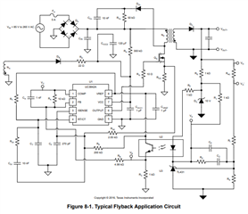
I made the circuit as shown on the circuit schematic below,

When I checked the output of the circuit, the voltmeter shows exactly 15.1 V (RMS).
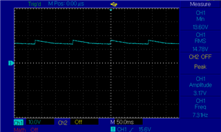
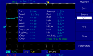
And when I connected the output of the circuit with my oscilloscope, I see that the RMS voltage is the same as the multimeter shows, but there are more than 4v fluctuating ripple between 13v to 16v.
Here are some shots from my scope.
I also measured the reference pin of TLV341 using multimeter, and it is exactly 2.5v.

I measured Vref pin of UC3845B using the oscilloscope, and It was fluctuating from 4.2v to 6v, but on the datasheet you provided it says it should be exactly 5v.

How can I make the Vref pin exactly 5v ? Also, how to solve the very high ripple on the output of the circuit and make the output as rock solid DC?

Thanks in advance

  • Hello Zaim,

    Here are a few improvements you can make.

    • It is not necessary to place a capacitor across the optocoupler. Remove C20 entirely.
    • The input current to Vref is quite high when you use a 1k resistor. Decrease the input current by replacing R3 with a 5k resistor.
    • C10 should be 1uF as shown below in the datasheet on page 26.

    Regards,

    Jonathan Wong

  • Hi Mr Jonathan,

    I removed C20 capacitor entirely from the circuit and I changed R3 with 5k resistor.

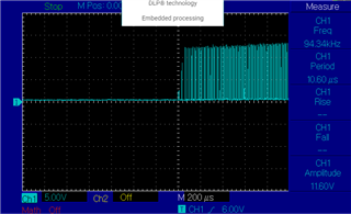
    This is the result of the output of the circuit

    and also I noticed that after doing these improvements there is a noise sound started coming from the transformer while it is working as shown below


    **not: because of the PCB is coming very late from China, we carefully test our circuit first on the lab.

    What are your recommendations to make this output voltage 15v steady as rock solid DC?

    Thanks in advance
    Sincerely,

    Zaim.

  • Hi Zaim,

    Jonathan is at a conference for the next few days so I will reply for him.

    When the regulator is switching it looks like it is operating near the correct frequency.

    1) Send a picture showing the gate pulses at 5us/DIV or 10us/DIV.  Use 20 MHz BW limit.  Measure the frequency with cursors, if you have them.

    2) Send a picture showing the gate pulses at longer time base, maybe 50us/DIV or 200us/DIV.  Is the regulator sending bursts of gate pulses?

    3) Send a picture showing the COMP signal.  Do this with offset and a low V/DIV and long enough time base so we can see if it is moving up and down.

    4) What is the load when you're making these measurements?

    Eric

  • Hi Mr Eric , thank you for your answer.

    1) Send a picture showing the gate pulses at 5us/DIV or 10us/DIV.  Use 20 MHz BW limit.  Measure the frequency with cursors, if you have them.

    2) Send a picture showing the gate pulses at longer time base, maybe 50us/DIV or 200us/DIV.  Is the regulator sending bursts of gate pulses?

    3) Send a picture showing the COMP signal.  Do this with offset and a low V/DIV and long enough time base so we can see if it is moving up and down.

    and here is the output voltage of the circuit


    4) What is the load when you're making these measurements?

    I used resistance load 100Ω 

    note**

    after doing what Mr. Jonathan suggested

    It is not necessary to place a capacitor across the optocoupler. Remove C20 entirely.

    the transformer started making noise as the video above.

    when I put C20 capacitor again the noise went away

    I also removed C13,C14 and C9 and added 2200uf 35v capacitor in place of these capacitors.

    ***

    sincerely,

    thanks in advance.

    Zaim

  • Hi Zaim,

    You shouldn't need capacitor C20.  It slows down the control loop and is one of the root causes of the issue you originally reported.

    The control method you implemented has 2 issues:

    1) The control topology used around the TL431 is Type-I (integral only).  This has no mid-frequency gain and is extremely slow.  TI strongly recommends a Type-II control topology to add some gain to the loop and have good bandwidth (i.e. speed).

    2) FB pin is grounded and opto-coupler alone is trying to control the COMP pin directly.  TI recommends connecting the error amplifier (FB and COMP pins) to form an inverting amplifier and add a small capacitor to add a roll-off at high frequency.

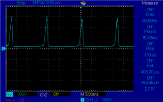
    When COMP swings up and down it results in bursts of gate pulses.  The frequency of the bursting is what you are hearing from the transformer.  COMP should be relatively consistent at some DC voltage and the gate pulses should not stop for a long period of time.  At light load the flyback will skip some pulses, but not have extended time with no pulses.

    COMP swinging wildly from low to high

    Burst of gate pulses

    COMP should not swing up and down like this (~0V to 3V).  When COMP looks like this it causes bursts of gate pulses.  From this waveform I can tell the gate is bursting on for ~2ms, then shutting down for about 14ms.  The on/off frequency of these bursts is 62.5 Hz.  I think this is the noise you hear from the transformer.

    The best way to resolve your issue is to use TI's recommended application circuit shown in the UC3845A datasheet (see below).  Note the way the TL431 is setup (Type II), how the opto-coupler is biased, and the use of the error amplifier (FB and COMP pins).  Also, the UC3845A has a terrific detailed design procedure on how the determine the component values.

    This flyback configuration has been used successfully in numerous designs for many years.

    Regards,

    Eric

  • Hi Mr Eric,

    I appreciate your kind and valuable support ,

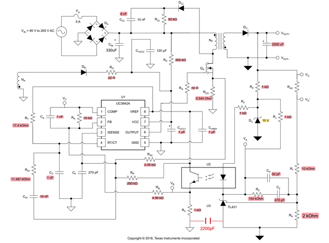
    As you recommended I made a new design according to the TI references design in the datasheet , I did all the calculation by suing all the formula in the datasheet you referred above and the values are given in red color in the circuit diagram below.

    After I made this circuit on the lab I noticed that the output of this circuit is fluctuating between 10v and 15v as shown on the video below.

    what do you think the problem comes from ?

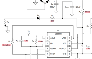
    note**I tried to disconnected Db diode from the transformer and supplied external 15v DC voltage to Vcc directly , and the output of the circuit was pretty good and clean 15v without any fluctuation.

    sincerely,

    ZAIM. 

  • I noticed you did not highlight the 120uF capacitor on VCC (CVCC2).  Do you have it?

    Eric

  • Yes I have all the components shown on the circuit above ,

    I only highlighted the components that I calculated my self using the equations on the datasheet above.

    I used the other nonhighlighted components with their recommended values. 

  • If you remove DB diode and drive VCC pin from external supply at 15V then everything is OK?

    Use your 'scope to compare signals (COMP, ISENSE, GATE, VREF...) with external 15V supply at VCC to the case using the auxiliary winding.

    Eric

  • One last thing, if you're using the UC3845 then the duty cycle is limited to 50% and you don't need slope compensation.  If this is the case then you can remove RS1 and CS1.

  • Hi Mr. Eric,

    If you remove DB diode and drive VCC pin from external supply at 15V then everything is OK?

    Yes, Without connecting load and supplying an external 15V at VCC PIN, I get a clean 15VDC output.

    Use your 'scope to compare signals (COMP, ISENSE, GATE, VREF...) with external 15V supply at VCC to the case using the auxiliary winding.

    Here are the waveforms I captured by connecting a 50Ω and 1kΩ load.

    ********************************************

    FOR 50Ω LOAD

    ******************************************

    A. EXTERNAL SUPPLY TO VCC PIN

    1. OUT PIN (MEASURED AT MOSFET GATE PIN)

    2. VCC PIN

    3. VREF PIN

    4. COMP PIN

    5. FB PIN

    6. ISENSE PIN

    7.  RT/CT PIN

    8. SMPS OUTPUT VOLTAGE

    ___________________________________________________________

    B. AUXILIARY WINDING

    1. OUT PIN (MEASURED AT MOSFET GATE PIN)

    2. VCC PIN

    3. VREF PIN

    4. COMP PIN

    5. FB PIN

    6. ISENSE PIN

    7.  RT/CT PIN

    8. SMPS OUTPUT VOLTAGE

    *****************************************************************************

    FOR 1KΩ LOAD

    ******************************************************************************

    AUXILIARY WINDING

    1. OUT PIN (MEASURED AT MOSFET GATE PIN)

    2. VCC PIN

    3. VREF PIN

    4. COMP PIN

    5. FB PIN

    6. ISENSE PIN

    7. RT/CT PIN

    8. SMPS OUTPUT VOLTAGE

    Note:

    -The IC used is UC3842 as in the design above.

    -when I used 50ohm load resistance I noticed that the output voltage is relatively stable with small ripples,

    on the other hand when I used  >100ohm load resistance I noticed that there is a voltage fluctuation.

    What is your recommendation to solve this issue and make the output voltage stable?

    Thank you very much.

    Sincerely,

    ZAIM

  • Hi Zaim,

    If you want it to work better at very light load you have to reduce the 2200uF output capacitance.  This large output capacitance can hold the voltage for a long, long time.  However, the VCC pin only has 120uF so its voltage decays relatively quickly.

    It's a balance between the Vout capacitor and VCC capacitor.  Try using an output capacitance of 220uF at light load.  At the same time increase the VCC capacitor.

    Flyback regulators have a MINIMUM LOAD.  You need to decide what this minimum load is.  Obviously, 1k is too low.

    Eric

  • Hi Mr Eric,

    I added another 2200uF at the output to make the total capacitance there 4400uF and also,

    I tried using 220uF at the output and in the same time increased the CVCC2 capacitor I used 220uF.

    But the results are the same with light load (I tried diffrent loads from 100ohms util 1kohms) .

    The Rcs resistor should be 0.5 Ohm,but Iam using 0.470ohm, 

    Is that occurs any problems?

    Flyback regulators have a MINIMUM LOAD.  You need to decide what this minimum load is.  Obviously, 1k is too low.

    When using1K resistor  it takes A=15/1000=15mA.

    Normally how you  decide the minimum load ? 

    This circuit should give output of 15v 3A.

    Why when I add 90ohm or less resistance load  on the output , the output voltage is optimized and stable on 15v without any fluctuating on the voltage? 

    But when adding higher resistance (more than 100ohm) the output is fluctuating between 10v to 15v or 5v to 15v ?

    Is there is any problems on the feedback loop?

    Thanks in advance.

    Sincerely, 

    Zaim.

  • Hi Zaim,

    Why do you keep increasing the output capacitance?  In general, if a switcher is operating normally the output voltage ripple may be reduced by increasing the output capacitance.  In your light load case the regulator is NOT operating normally.  The VCC voltage is decaying and the controller is repeatedly turning off, then on, as VCC goes down and up.  The light load plots you sent are at seconds per division!

    Flybacks can operate from about 10% load to 100% load.  In your case 50 ohms equates to 300mA (10% load).

    I recommend you add a dummy load, say 75 ohms (3W), to the output.  This will make it regulate at "no load".

    Regards,

    Eric