This thread has been locked.

If you have a related question, please click the "Ask a related question" button in the top right corner. The newly created question will be automatically linked to this question.

BQ76952: Set ALL_FETS_ON then working about DSG and CHG MOSFET off after

Part Number: BQ76952
Other Parts Discussed in Thread: BQSTUDIO,

Hello Sir:

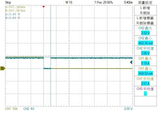
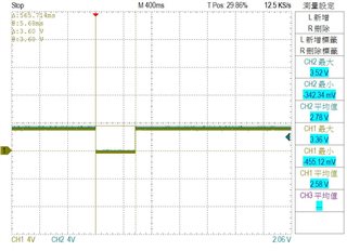
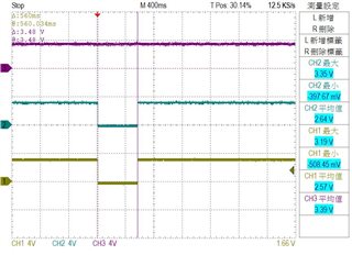
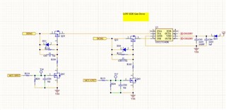
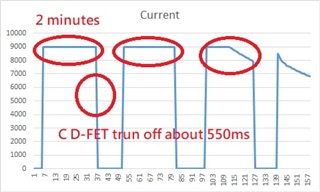
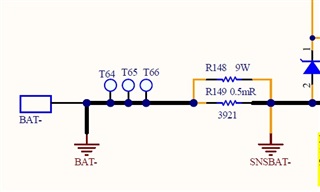
As the title, we set the mosfet on by using ALL_FETS_ON command, but after charging or discharging.

CHG and DSG MOSFET will turn off, but I cannot find reason.

This case happened on MCU firmware, didn't use BqStudio, we log all registers and flash memory for you checking.

Please refer attached files.

If there are not clearly or not enough for checking root cause.

Please let me know which register or flash memory you wanted, I will check back for you.

Looking forward your feedback.

Thanks a lot.

BQ76952_Data_Memory_Table_After_Charge.xlsx

BQ76952_Data_Memory_Table_After_Discharge.xlsx

datalog_202210071348_Cha_QQE.XLSX

datalog_202210071424_Dis_OCD_SCD.XLSX

  • Hi Statham,

    Our applications team is at the Battery Management Seminar the next two days, but we can take a look at these files on Thursday and get back to you. Is the FET_EN bit set in the Init Mfg Config register or has the FET_ENABLE command been sent to enable autonomous FET control?

    Best regards,

    Matt

  • Hi Matt,


    Init Mfg Config : FET_EN = 1.

    Before starting charging, send the command ALL_FETS_ON 0x0096.
    After charging for about 2 minutes, DDSG and DCHG will pull Low for 550ms, and there is no trigger protection at this time.

    Thanks.

    Benson

  • Hi Benson,

    I do not see anything in the files that explains this behavior at first glance. I will take a closer look tomorrow when we are back in office. If you have any other information that may be helpful for debug, let me know. Is the REG1 voltage stable during this event?

    Regards,

    Matt

  • Hi Benson,

    Can you share your schematic? Do you monitor the REG1 voltage when this behavior is occurring?

    Regards,

    Matt

  • Hi Matt,

    When the problem occurs, REG1 is stable.

    I have tried setting the DDSG DCHG as a GPO and controlling it through the MCU, there will be no such problem.

    But I need BQ hardware to protect SCD and OCD, so I still need to set it to DDSG, DCHG.

    Thanks.

    Best Regards,

    Benson

    CH1 DDSG, CH2 DCHG, CH3 REG1

  • Hi Benson,

    Looking through your log file (the one labeled OCD_SCD), I see that OCD1 and SCD are causing the DCHG and DDSG pins to toggle. So I am confused about what the problem is - this is the behavior you expect, right? For the charging log file, I cannot find the reason why the FETs would turn off. At one point the WAKE bit reads low - is there any type of reset occurring? 

    Matt

  • Hi Matt,

    My problem is that when it is set to DDSG DCHG, in the charging state, the charging interruption occurs every two minutes, at which time the DDSG DCHG will be turned off for about 550ms.
    I can't figure out why, and no protection has occurred, so I'm asking for help.

    Thanks & Best Regards,

    Benson

  • Hi Benson,

    What is your sense resistor value? Can you try to disable the SCD protection (or maybe disable all protections) to verify that this is not caused by a protection triggering?

    Regards,

    Matt

  • Hi Matt,

    I tried turning off all protections and the problem still occurs.

    The following values ​​are all set to 0x00.

    EnabledProtectionsA 0x9261
    EnabledProtectionsB 0x9262
    EnabledProtectionsC 0x9263
    CHGFETProtectionsA 0x9265
    CHGFETProtectionsB 0x9266
    CHGFETProtectionsC 0x9267
    DSGFETProtectionsA 0x9269
    DSGFETProtectionsB 0x926A
    DSGFETProtectionsC 0x926B
    ProtectionConfiguration 0x925F

    Thanks & Best Regards,

    Benson

  • Hi Benson,

    Okay, so this eliminates the possibility of a protection causing this behavior. Is there any chance the microcontroller is sending commands that may cause the FETs to disable? The time period doesn't really match anything that would make sense for the monitor device.

  • Hi Matt:

    I checked again their registers setting.

    1. DCHG and DDSG pin config, their setting is AA, if change to A2 will be better or not?

    2. FET Options and ChgPumpControl are 0E and 01, if change to 26 and 0 will be better or not?

    3. Their circuit is using low side FET, would you please recheck registers which setting dose not meet low side FET requirements?

    I will send their schematic for you by message.

    Looking forward your feedback.

    Thanks a lot.

  • Hi Statham,

    I think the DCHG and DDSG pin settings are okay. I think they should try to set CHGPumpControl to 0 because I see in the schematic you sent that this pin is shorted to the BAT pin (no charge pump capacitor). Their FETs are configured in series, so the [SFET] bit should be set in the FET Options register.

    So FET Options should be set to 0x07.

    On the schematic, I also notice that the capacitor on the REGIN pin is 10nF. This is outside of the datasheet range - it should be 22nF.

    When they measure the waveforms, are they measuring the signals right at the DCHG and DDSG pins of the device? There are other circuits between these pins and the FET gates, so it would be good to confirm.

    Best regards,

    Matt

  • Hi Matt:

    Customer set FET options to 0x07, CHGPump set to 0 and changed the REGIN cap to 22nF, but it's not useful.

    And there has no other circuits between DCHG and DDSG of the device, DDSG connected to Q20 pin2 and DCHG connected to Q21 pin 2.

    Can you try their settings on your side? 

    6332.BQ76952_Data_Memory_Table_After_Charge.xlsx

    The other, one requirement and one question.

    1. do you have a guide line to talk more about DCHG and DDSG pins function? we need to have a work around way to fix this issue.

    2. when normal mode, is it possible to change DCHG & DDSG to alternate mode --- as DDSG and DCHG function or GPIO mode?

    Anything you think which may be a problem, please kindly let us know.

    Looking forward your feedback.

    Thanks a lot.

  • Hi Statham,

    I am testing now on my EVM with their settings. I cannot observe the same behavior - DCHG and DDSG are always enabled. Is it possible there are commands from their microcontroller that could explain the behavior? Can they disconnect the microcontroller to verify the behavior does not change?

    DCHG and DDSG should follow the CHG and DSG pins. The only difference is with the precharge and predischarge functions - this is explained in the Low Side FETs application report. DDSG combines the PDSG and DSG outputs (if either is asserted, PDSG is asserted) and PCHG combines the PCHG and CHG outputs.

    The only way to change the mode of the DDSG and DCHG outputs to general purpose output is to change the DCHG Pin Control and DDSG Pin Control register settings. They should not be changing register settings during normal operation though because FETs are disabled while in CONFIG_UPDATE mode.

    Best regards,

    Matt

  • Hello Matt:

    DDSG and DCHG issues has been fixed, root cause is communication failed over 60 times, then MCU will re config SET_CFGUPDATE, then DDSG and DCHG will pull low by that processes.

    But we have a question about FET Options set 0x07.

    When set 0x07, FET status value is 0, and if OCD1 or SCD happened that DDSG will not change to low.

    But if we set 0x0F, when OCD1 or SCD happened that DDSG will change to low.

    Is it possible?

    Please let us know your reocmmendations.

    Thanks a lot.

  • Hi Statham,

    The [FET_CTRL_EN] needs to be set to '1' or the timing will not be correct on the OCD Delay or SCD Delay. I think another user also observed this issue in the past and I confirmed it by testing the behavior on an EVM. I think we were planning to clarify this in the TRM, but I will check.

    Best regards,

    Matt