This thread has been locked.

If you have a related question, please click the "Ask a related question" button in the top right corner. The newly created question will be automatically linked to this question.

UCC2808-1: two questions about how to use

Part Number: UCC2808-1
Other Parts Discussed in Thread: TL431, LM311, LM211, LM211-Q1

Hi Experts,

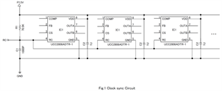
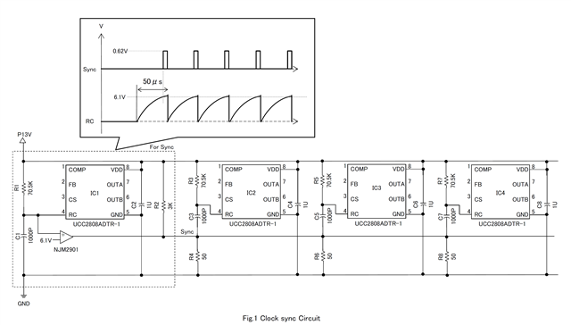
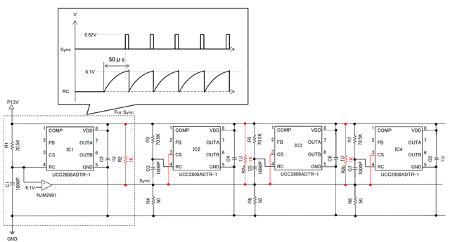
I have two questions about how to use the UCC2808-1.

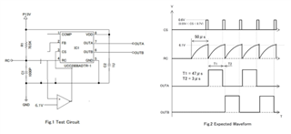
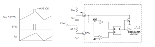
First, please tell me about the duty ratio adjustment method (circuit).
For example, what kind of circuit design would be used when the duty is 47%?

Second, I want to ground COMP and turn off the outputs (OUTA, OUTB).
Hypothetically, is it a problem to ground COMP for many months with power on?

I hope to receive your advice. Thank you so much.

Kind regards,

Gerald

  • Hi,

    The duty is adjusted by COMP voltage - you can use any approach to adjust COMP voltage. Typically, in a closed-loop and DC-DC isolated converter, COMP is adjusted by sensing converter output voltage and through TL431 and opto-coupler, and an example is shown in the data sheet on several pages such as on page 1 and on the page of Typical applications. 50% duty is the maximum duty OUTA or OUTB can make. 47% is something before reach 50% when the feedback loop possibly to adjust to regulate the converter output voltage.

    COMP can be pulled down to GND forever and no problem on the IC when it is powered on.    

  • Hi Hong,

    Thank you for your answer. Please tell me about duty-change.
    Actually, when the COMP voltage is 2V at open, how many volts should COMP be to fix the duty at 47%?
    Do you use FB? Is FB grounded?
    Kind regards,
    Gerald
  • Hi,

    If ground FB, then COMP would be at its max high then the duty is 50% in theory but practically typical 49% based on the data sheet. 47% is achieved when COMP almost reaches its max high. Due to the tolerance, one sample achieve 47% does not make another 47%.  

  • Hi Hong,

    I appreciate your support. I still received a feedback from customer and hope to receive further advise.

    We are not sure how to change the duty cycle ratio. Let me ask four questions. Please check the attached document for details.

      Q1.Can I get the expected waveform with this IC?

     Q2.Can I get the expect waveform(Fig.2) from the circuit in Fig.1?

     Q3.Please let me know the resistance values of R2, R3 and R4 when T1=47μs and T2=3μs.

     Q4. Is it ok to short the RC to stop it?(For synchronizing with multiple ICs)

    YN20221014-01_Inquiry about How to use the UCC2808A-1.pdf

    Thank you so much.

    Kind regards,

    Gerald

  • Hi,

    Q1.

    Yes, you can get the expected waveform with this IC.

    Q2.

    You need change your circuit, remove R2, R3 and R4, then short COMP to FB - this will set up the internal PWM comparator with threshold 1V. You need to add a saw tooth waveform to CS and sync that saw tooth waveform in each clock cycle to reach 1V in 47us. The RC clock will be set up for 50us see Q3.

    Q3.

    Based on your waveform the frequency = 20kHz (47us + 3us), so if you select C1 = 1000pF then R1 = 70.5k, please refer to Fig 1 of the data sheet. 

    The above can help to get to the nearby of what you specified. You would need to tune up to get the accuracy you need. Please note, the IC parameters have distributions, so when you use the same parameters of R1 C1 and CS saw tooth from 0 to 1V in 47us, you may not always get 47us + 3us, and most likely you can only get this from your tuned up device. 

    Q4.

    For clock sync, you need tie RC pin together from each IC to sync them together. Please note, RC peak is roughly 0.5 x VDD so each IC in sync needs to have same VDD.

    I am not understanding "to short the RC to stop it"?

  • Hi,

    On Q2, when short COMP to FB, COMP only can get 2V typical. So the PWM comparator threshold would be 0.91V. CS to COMP has a typical offset 0.8V. So CS saw tooth in each Clock should be from 0 to 0.11V with 47us. 

    But CS to COMP offset can be as high as 1.2V. If a device has such a parameter value, you won't get 47us. So to cover such a case, FB needs back to your circuit and design COMP voltage to make the PWM comparator threshold 1.2V, COMP = 2.64V, since FB = 2V, then you can calculate R2, R3 and R4. For this particular device, CS saw tooth would be from 0 to 0.4V in 47us, in order to get your specified waveform.

    But after you do this, and when you have another device which has CS to COMP offset lower than 1.2V, then the CS saw tooth would need longer time to reach 1.2V PWM threshold. Then this device won't produce your waveform accurately.

    So back to Questions, this device can produce the expected waveforms but you would need to tune up each device as due to the parameter variations, you cannot use one set design values to cover from device to device.

  • Hi,

    There is another approach that can provide a bit better solution.

    You would need to add a comparator and set up 6.1V as threshold. So when RC reaches > 6.1V (assume VDD = 13V), the comparator output change to > 0.5V, which will trigger Peak current comparator to turn off OUTA or OUTB. So this way can make 47us on and 3us off in theory. But again, CS peak comparator threshold is with min 0.45V and max 0.55V. So you may not get accurate 47us and 3us. But this approach should have better accuracy than the previous ones.

    Since the threshold can be as high as 0.55V, so the external comparator output needs > 0.55V, but < 0.7V which is a threshold to trigger over current threshold and will trigger soft start to interrupt the operation.

  • Hi Hong,

    We appreciate your support.

    Could you tell me about your suggestions use a comparator?

    Please, tell me the model number of the recommended comparator.

    Is the output of the comparator regulated to 0.6V (0.55V<CS<0.7V) with a resistor divider?

    I added the CS waveform that I imagined. Do you match?

    Additional question, Is it okay if I ground the RC while the power is on?

    (The purpose is to prevent unnecessary operations while the system is on standby (several months).)

    Thank you for your consideration.

    Best regards,

    Gerald

  • Hi,

    On the voltage comparator, something like LM311 or LM211 or LM211-Q1 can be used depending on your application temperature range. If you use a different part, please pay attention to the speed. LM311 has speed < 0.2us so it is ok in your applications. So please use speed < 0.2us parts.

    Yes, the comparator output has to be within 0.55V and 0.7V to trigger max peak current threshold and not to trigger the over current limit. You can use a resistor divider if this range can be achieved.

    Yes, your CS waveform is correct.

    If you want to disable the IC, the datasheet suggestion is to pull down COMP pin. 

  • Hi,

    Thank you for your prompt reply. About the duty adjustment, the customer said that he will check it later.
    He also wanted to ask you another question.

    Could you tell me how to synchronize the clocks of multiple ICs.

    Q1. Is the circuit shown in fig1 correct? Could you give me a sample circuit

    Q2. When I tried using 3 ICs, only one IC could output(OUTA,B). Is there something missing in the circuit?

    Q3. Is it okay to ground the RC for about one cycle to reset (restart) the RC?

    Q4. Are there any restrictions (precautions) on the circuit when synchronizing 6 ICs?

    Thank you for your consideration.

    Best regards,

    Gerald

  • Hi,

    Q1, Q2

    If you look at the datasheet, Fig 5, on page 8, you can see to generate clock pulses, RC needs change bellow 0.2V and above VDD/2. Each device has some difference on VDD/2 threshold (see table on page 4, VDD/2 means, 0.44VDD to 0.56VDD), so the device with the minimum would produce clock ok but the remaining cannot as the saw tooth does not reach their VDD/2. So, you need to provide an external pull-up circuit to force each IC RC above VDD/2 a bit, say 0.56VDD or slightly higher. 

    Q3,

    If ground RC for cycle is ok. But if you want to disable the IC for long time, the datasheet suggests pull-down COMP.

    Q4,

    No restrictions on IC side for how many in frequency sync. 

  • Hi,

    Thank you for your prompt reply. And customer has successfully adjusted the duty using the comparator.

    But he still hasn't solved the sync issue. So, I have a few questions.

    Q1. For example, is the synchronous circuit (three ICs) OK in Figure 1?

        (I am using the same IC for "sync". Is it OK?)

    Q2. If not, how should Sync be made in particular? Could you give me a sample circuit?

    Q3.  Is it possible to adjust the duty by creating a synchronous circuit?

    Thank you for your consideration.

    Best regards,

    Gerald

  • Hi,

    Q1.

    The pull-up needs to apply to every IC. In your circuit the very left will start a new cycle earlier or later than the other three depending on the very left one VDD/2 tolerance.

    Q2.

    I suggest you make an external sync circuit, or use the very left one to produce the sync, so the remaining 3 are ok to sync'ed.

    Q3.

    If your CS reset each cycle after sync, then the duty is from the sync till CS reaches above 0.5V. In this sense, the duty is not adjusted if the CS has a same slope. If you change the CS slope faster, the duty will be smaller, then your off time will be longer if you keep the sync clock same frequency. 

  • Hi,

    Thank you for your prompt reply.

    I reviewed the circuit diagram from the answer.
    (Corrections are in red)
    Is my understanding correct?

    Thank you and kind regards,

    Gerald

  • Hi,

    CS should be with a saw tooth and peak at 0.55 to 0.65V. Your circuit cannot achieve this.