This thread has been locked.

If you have a related question, please click the "Ask a related question" button in the top right corner. The newly created question will be automatically linked to this question.

BQ76952: BQ76952 Interface

Part Number: BQ76952

Dear Sir/Madam,

I am working on BMS for Telecom Battery (48 V / 100 Ah ) with 15/16 Cell LFP.

I am using BQ7695202 SPI bms chip with Isolated Communication and try to control from mcu and bms afe using OR gate.

Please check the attached schematic and share your feedback.Let us know to us for any other information
OGO_BMS-MOSFET_PARALLEL.pdfMainboard-BMS AFE.pdf

  • Hi Ramesh,

    After looking at your schematic, I noticed quite a few issues.  I recommend watching this video on building a schematic with the BQ76952: Creating the Schematic for BQ769x2 Battery Monitors - YouTube.

    Pertaining to the main board:

    Since you are using the BQ7695202 with SPI communication, you should not be using the BQ7695202, since this device is for I2C communication.  If you would like to use SPI, please use the 03 or 04 version of the device.

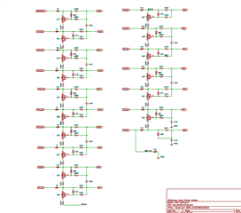
    There is also an issue with your cell connects.  I noticed that 13-16 are connected correctly, but 0-12 are not connected to their corresponding pins.  The BQ76952 supports random cell connections, meaning cell 1 could be connected at a point in time after cell 12, for example, but cells in the stack cannot be connected to just any VC pin.  For example, cell 7 cannot be connected to VC pin 1. 

    Please read Section 16.3 Random Cell Connection Support of the data sheet linked here: BQ76952 3-Series to 16-Series High Accuracy Battery Monitor and Protector for Li-Ion, Li-Polymer, and LiFePO4 Battery Packs datasheet (Rev. B) (ti.com).

    Additionally, the REG18 capacitor should be 2.2uF, and REGIN should have a 22nF capacitor without a resistor between the pin and the capacitor.  You are also using REG18 as a pullup on the Alert pin, and that is bad because REG18 should not be used for any external circuits.

    REG1 should not have a resistor between the pin and the capacitor, and I would need to see the values for the rest of the components in your circuit to know if there were other issues.  Finally, TS2 shouldn't be connected to a thermistor if you need to use SHUTDOWN mode at all. 

    Pertaining to the parallel FETs:

    You may need to have to add additional circuitry on the output of the charge FET driver to prevent this from going too negative if your low-side driver cannot handle voltages that could become too negative. More information can be found in Figure 2-1 and Section 5 of the application note linked here: Using Low-Side FETs with the BQ769x2 Battery Monitor Family (Rev. A) (ti.com).

    You do not need a zener for every FET in parallel, one should be enough, and the gate-source resistors should be before the gate resistor (R168 before R166, R479 before R178, etc..)

    Best,

    Andria

  • Hi Andria,

    Thank U for sharing your feedback,

    I have modify the schematic as suggested by you, Please check the attached schematic and share your feedback.Maiboard-BMS AFE.pdfMaiboard-Cell Interface.pdfMaiboard-MOSFET_PARALLEL.pdf

  • Hi Ramesh,

    I see that you have addressed most of the issues I included in my last message.  Just a couple more things:

    • I see that REG18 is now connected to V18, but I didn't see where V18 leads.  I just wanted to check that you are following the datasheet, which states that: The 1.8-V LDO (REG18) provides a regulated 1.8 V supply voltage for the device's internal circuitry and digital logic. This regulator uses an external capacitor connected to the REG18 pin, and it should only be used for internal circuitry.
    • You have not addressed the issues with the parallel FET configuration.  Please revisit those statements from my earlier post and refer to this app note: Using Low-Side FETs with the BQ769x2 Battery Monitor Family (Rev. A) (ti.com).
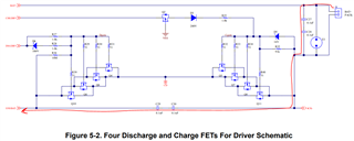
    • The ESD protection you have implemented for your parallel FETs may need some adjusting.  The 100 nF capacitors in series are used to direct high voltage ESD pulses around the FETs to avoid damaging them.  I have shown the desired path for ESD current with a red arrow on Figure 5-2 as an example to illustrate how you should configure your capacitors to protect your system.  Please ensure that your capacitors are laid out in a similar way.

    Best,

    Andria

  • Hi Andria,

    Please check our comments against your suggestion

    • I see that REG18 is now connected to V18, but I didn't see where V18 leads.  I just wanted to check that you are following the datasheet, which states that: The 1.8-V LDO (REG18) provides a regulated 1.8 V supply voltage for the device's internal circuitry and digital logic. This regulator uses an external capacitor connected to the REG18 pin, and it should only be used for internal circuitry---Not used this pin in our schematic ,add a test point on this pin.
    • You have not addressed the issues with the parallel FET configuration.  Please revisit those statements from my earlier post and refer to this app note: Using Low-Side FETs with the BQ769x2 Battery Monitor Family (Rev. A) (ti.com).--- I have checked the documents(Reference manual ) and modify the schematic


    7288.Maiboard-MOSFET_PARALLEL.pdf

    Zener Diode and Resistance has been removed as shared by Reference manual.

    Please suggest the Component value also.

  • Hi Ramesh,

    Thank you for clarifying that V18 is a test point.  That should be okay.

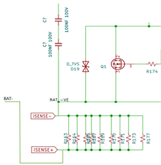
    Your current sense resistor configuration appears problematic as well.  The resistor network should not be in parallel with the main path for current flow, and SRP/ISENSE+ should be on the BAT- side.  Please adjust your sense resistor to a configuration similar to the image below:

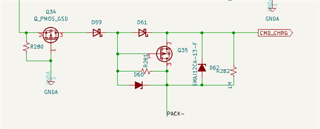
    I think the rest of your schematic looks okay, except for the portion with ESD protection from P+ to BAT -ve.  This is unnecessary, and you can remove it.  I will attach an image of the section below.

    Best,

    Andria

  • Hi Andria,

    Thanks for your support and i have been observed the Issue0284.Maiboard-MOSFET_PARALLEL.pdf and corrected, Please have a look again.

  • Hi Ramesh,

    I recommend following the image I created in my last post.  Although you have changed the sense resistor configuration, it should be located after the parallel FETs and ESD protection network.

    Best,

    Andria

  • Hi Ramesh,

    It looks like you have addressed the issues in your latest schematic.

    Best,

    Andria