- Ask a related questionWhat is a related question?A related question is a question created from another question. When the related question is created, it will be automatically linked to the original question.
This thread has been locked.
If you have a related question, please click the "Ask a related question" button in the top right corner. The newly created question will be automatically linked to this question.
Hi,
We have a design for a stacked battery pack BMS system using the BQ76PL536A integrated circuit.
Most of the time it is working, but every once in a while we have one of the BQ IC's fail (small burned mark in one corner) when the circuit is plugged in, or sometimes if the battery pack is connected to a load without a precharge resistor and a high current flows in the pack.
We think this may be due to the voltage reference connections between the sets of 6 cells for each BQ IC, and we need to understand the N-S stacking for the voltage references/current return paths. (We understand the communications signals just fine, and that they are "current signals"-- but the datasheet does not explicitly describe how/where the current return path for those signals is to be implemented) the voltage reference seems likely to be where the current return path is, but we don't know how that works and what connections are required to allow for that return current.

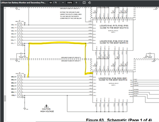
In the data sheet (bq76pl536a.pdf) figure 63 the schematic shows a connection between Cell 6+ and Cell 7- over at the pack, but then also another connection between cell0 on the 2nd BQ IC and between 1-VBAT on the 1st BQ IC. That set of connections is quite confusing, on our board we connect cell 6+ directly to 1-VBAT to power the first BQ IC instead of routing the voltage back and forth across/between BQ IC's.
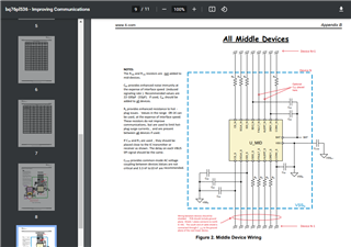
And then on the BQ IC wiring recommendations document "Improving communications with the BQ73PL536" SLUA562 that document in figure 2 does not show any voltage reference connecting between the two daisy-chained BQ IC's.
So is that voltage connection between the daisy chain required, or not? And if so, what is the correct way to implement it given that the pack itself connects Call 6+ to Cell 7- in the high powered wiring.
Hi Michael,
Have you seen this reference design connecting multiple devices together? https://www.ti.com/lit/ug/tidub04/tidub04.pdf?ts=1599505715930
Also have you considered bq79606a instead? It is a more rich featureset 6S monitor from this older device and more robust communications across devices.
Regards,
Taylor
Thanks Taylor, in the long term we'll consider the alternative IC.
The reference design is also useful for seeing how designs might be put together, but is still not instructive as to how things actually work, and I find debugging systems much easier when I understand how they work.
In the meantime, can you explain where the "return current" flows for the SPI signaling between the two devices? I've pored over the data sheets and it isn't explicitly stated anywhere that I can see, and not 100% obvious since the grounds aren't connected. No actual schematics (or pseudo-schematics) of the SPI transmitter/receiver is presented, so it's a bit hard to figure out where the return current would flow.
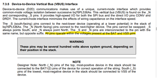
The text copied from the data sheet below seems to suggest the that VSS connection on the higher potential device to the BAT terminal on the lower potential device is the signaling current return path. Does this sound correct?
If that is the current return path, then my question relates to how to make that connection given that their is a high power, high current connection between the top cell of the lower sub-pack and the bottom of the next pack, and how to make sure that during connecting up the system that high current path does not accidentally flow onto the board where VSS (bottom cell, upper pack) and VBAT (upper cell, lower pack) might also be connected in a parallel path...
Thanks,
Mike

Mike,
This is an isolated differential signal between devices so there is no shared gnd between the two devices, rather the signal is generated from one device common to respect to its local gnd and transmitted across the lines to the higher device which would then interpret the signal differentially. This is a similar concept to RS 485 or CAN transcievers. Sometimes we see benefits to AC coupling the gnd paths with small caps to avoid noise interrupting the signal quality.
Regards,
Taylor
Hi Taylor,
Yes I understand that. As I mentioned above I am completely aware that this is a current signal and not a voltage signal, which allows for the different IC's to be at different ground references.
But to use your example, in RS485 there is a differential pair. (Although RS485 is still a voltage signal, just a differential, so not a 100% analogy)
I think a more apppropriate analogy might be in industrial signaling there is a 5-20 mA current loop standard that removes any common voltage reference.
In all of these cases, there is a *loop*. For the SPI current transmitter to send a 1 mA "1" signal, that 1 mA must "come back" the IC somewhere. (Kirchoff's current law)
So my question is, where is the current return path when the transmitter sends a current signal to the receiver on the "other" BQ IC, where does that current return path back to the transmitter IC?
Thank you!
Mike
Mike,
I believe this app note may answer your questions: https://www.ti.com/lit/an/slua562/slua562.pdf
Regards,
Taylor