This thread has been locked.

If you have a related question, please click the "Ask a related question" button in the top right corner. The newly created question will be automatically linked to this question.

TPS59650: Schematic Design Review

Part Number: TPS59650
Other Parts Discussed in Thread: TPS51650

Hello,

Greetings of the day!TPS59650RSLT.pdfTPS51650 Calculator DCR Sense_10kNTC QC_Aug1_2011_01_Nov22.xls

I am working on Power Section Design of Intel Atom E3826 using discrete IC's & Components (without PMIC). In the design, two core supplies are required for Atom as follows-

CORE_VCC:  4A @ 1.0V

UNCORE_VNN_S3:  10A @ 1.0V.

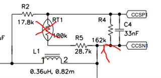
For the above requirement, I am using TPS59650RSLT from TI. This component has 3 CPU phases & 2 GPU phases. And, I have used 1 CPU (for CORE_VCC) & 1 GPU (for UNCORE_VNN). Kindly preview the attached schematic for the reference. 

Now, My doubts are- 

1) As I am Not using 2 CPU & 1 GPU phases, what should I do with their unused respective pins?

2) Are Bulk capacitors required for the output current 10A & 4A.

3) As I am following Spreadsheet "TPS51650 Calculator DCR Sense_10kNTC QC_Aug1_2011" for the reference, what Inputs should I take for the following sections-

3.A) Thermal Design Current (I_TDC_total)?

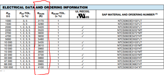
3.B) value of B value of DCR thermal compensation NTC and Resistance of NTC at 25C ?

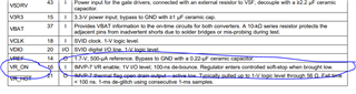
3.C) what is meaning of OSR/USR setting level at COCP-R and GOCP-R that is fixed at 1V & 1.6V?

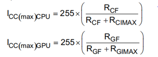
3.D) IMON voltage at Icc_max?

Please help preview the attached schematic & Design Spreadsheet for the reference- 

As, We have on-board space constraint, so please consider use of optimal components while reviewing the design. 

Thanks & Regards

Raj Kumar 

  • Hello Raj,

    1. Tie the unused phase CSP pins to V3R3, float unused CSN & PWM pins. Note that you must use the lowest-number phase on a given rail (disabling phase 1 will also disable phases 2 & 3, disabling phase 2 will also disable phase 3).

    2. I'd still recommend having a bulk capacitor, though it may not be necessary. You'd have to test that yourself. You could put a DNP cap on your test board and see if how the performance compares with and without the cap.

    3A. The I_TDC_total is the maximum RMS current the rail is expected to drive.

    3B. For thermal compensation, you can use an external NTC resistor in the compensation network. The B value will be specified in the thermistor's datasheet.

    3C. This might be something used internally by the calculator. If you change the OSR setting, the calculated COCP-R pinstrap resistors change.

    3D. I don't understand this question.

    Also, does your application require IMVP7? There's a lot more options that can fit in a smaller space if not required.

    Thanks,

    Travis

  • Hello Travis,

    Thank you so much the guide!

    1) I am using First phase of CPU for CORE_VCC supply and First phase of GPU for UNCORE_VNN_S3 supply. Is this configuration correct?

    2) Is it required to use DCR Sensing circuit for thermal compensation of 10A & 4A output current @ 1.0V?. If I can avoid using it then What would be the connections of CCSP & GCSP of first phase?.

    Please let me know if you any other remarks my shared schematic. 

    Thank You

    Raj Kumar

  • Hello Raj,

    1. That's the correct configuration.

    2. If you wanted to avoid temperature compensation, you'd connect CCSN & CCSP to a voltage divider across the inductor. In this example, you'd remove RT1 & change the value of R4. However, that will effect the current sense accuracy.

    Also, can you confirm if your application requires IMVP-7?

    Thanks,

    Travis

  • Hello Travis,

    Greetings of the day!

    Yes, My application requires IMVP-7 to support SVID interface. 

    I have one more doubt regarding VR_ON pin the Package. 

    As per datasheet, VR_ON comes under SVID interface with 1V I/O level. But I want to derive this pin externally (3.3V I/O level). Can I do so, as recommended Operating  conditions for VR_ON pin is given as 0V to 3.5V. 

    Thank You

    Raj Kumar

  • Hello Raj,

    Driving the pin at 3.5V shouldn't be a problem.

    Also, I should be able to complete the schematic review by the end of next week.

    Thanks,

    Travis

  • Hello Travis,

    Thank you for confirming the VR_ON I/O Voltage.

    Yes Please, I'll be waiting for your comments on schematic if any. 

    Thank You 

    Raj Kumar

  • Hi Raj,

    Apologies for the inconvenience, but I need to delay the schematic review. I should have the review complete by the end of Tuesday.

    Thanks,

    Travis

  • Hi Raj,

    Review is complete.

    TPS59650RSLT ti commented.pdf

    Thanks,

    Travis

  • Hi Travis, 

    Thank you so much for the schematic review & comments. 

    I wanted to clear one doubt from your comments on the schematic. 

    you have commented "MINIMUM IMAX CURRENT IS 20A (133mV)". What do you mean by that? Because I have calculated the IMAX current value using the formula given in datasheet, and it comes 4A (CPU), 10A (GPU). 

    Please elaborate your above comment. 

    Kindly refer your commented schematic from previous message. 

    Thank You

    Raj Kumar


  • Hi Raj,

    My concern is that the IMAX current cannot be set that low. I have contacted another internal person to confirm, and I'll get back to you by Wednesday (US time).

    Thanks,

    Travis

  • Hello Raj,

    IMAX cannot be set to less than 20A (133mV). I recommend you check with Intel to confirm if this causes an issue with IMVP-7 current reporting.

    Thanks,

    Travis