Hi All,
I'm designing a boost circuit based on the TPS40210 with the following specification:
| VIN | 15V |
| VOUT | 150V |
| VD | 0.9V |
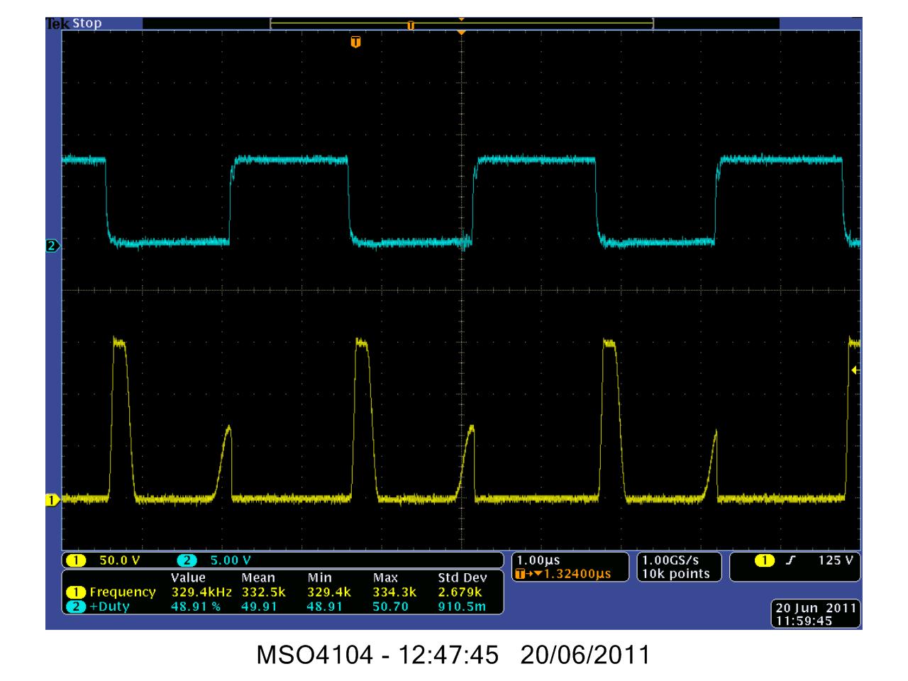
| FSW | 320kHz |
| L | 100uH |
| IOUT | 15mA |
The output current can vary from 0 to 15mA, so I've chosen to use discontinuous conduction mode. I have some questions regarding the required compensation network and the inductor current requirements, but first I'd like to give my calculations to see if they look sensible. (Equation numbers used below are those from the TPS40210 datasheet).
Here is the spreadsheet I used to make the calculations: 0513.TPS40210 DCM.xlsx
- The duty cycle is 0.64 (using equation 3)
- The critical output current is 22.38mA (equation 4) as this is greater than the required 15mA, control should stay in discontinuous mode.
- I've selected CT = 100pF and RT = 510K, this gives the 320kHz switching frequency.
- Based on Eqn 6, the sense resistor is 325mR, I've selected 330mR which gives a trip current of 25mA
- On time is about 2us (Eqn 11), which gives CIFLT = 100pF, RIFLT = 2K (Eqn 12)
- Using Eqn 57, RFB = 100K RBIAS = 470R
Inductor Currents
I'd like to calculate the inductor peak current. When in discontinuous mode are equations 34 & 39, still usable? From a different application note (SLVA061, Page 8) the peak inductor current is given as (VI x D) / (L x FSW), is this OK to use?
Compensation Network
I'm struggling quite a lot to get a complete grasp of calculating the required compensation network component values. If I understand correctly the situation is more relaxed in discontinuous mode. Are equations 22 to 29 still appropriate?
Switching Frequency
Are there any advantages in using a higher switching frequency? The equations suggest that a higher FSW forces the use of a lower inductance to maintain discontinuous mode. The load is actually a fast switching circuit (around 100kHz) that requires bursts of current every time it switches. Would a faster switching frequency improve the controllers ability to maintain the correct output voltage?
This is a lot of info and questions, so many thanks for your patience.
Thanks
Andy