This thread has been locked.

If you have a related question, please click the "Ask a related question" button in the top right corner. The newly created question will be automatically linked to this question.

Do we need to remove the GND shape underneath the inductor on the same layer,for good EMC performance

Other Parts Discussed in Thread: LM53635-Q1

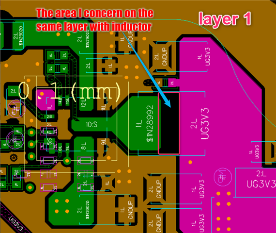
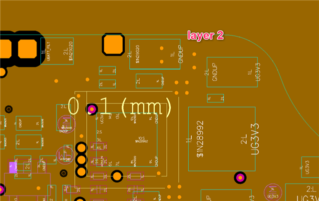
For DC-DC converter design in 4-layer PCB or 6-layer PCB( components on top layer,layer 2 is GND),do we need to remove the GND shape underneath the inductor on the same layer, for good EMC performance?if we don't remove the GND shape ,does it bing in the parasitic capacitance with inductor?

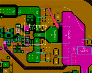
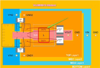
 in the layout example of  TI-LM53635-Q1 and TI-LM63635-Q1 datasheet, both no keep-out GND design under the inductor. as below  


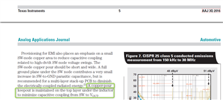
regarding to P6 of  "reduce buck-convertor EMI by minimizing inductive parasitics" as below. it recommends set a keep-out area on the top layer under the inductor.FYI

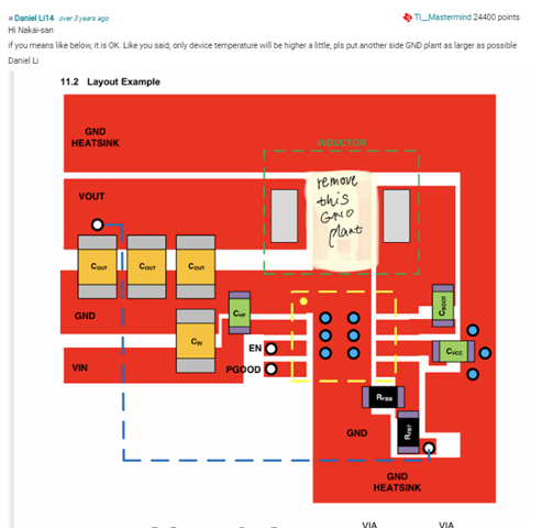
the answer as below link also suggest that design a keep-out area for inductor

LMR33630: Can GND plane located under Inductor be removed? - Power management forum - Power management - TI E2E support forums 

I don't know which design is good for EMC performance,and why?Waiting for your advice.Thank you.

  • Hi Chris,

    This is a controversial topic and there is no absolute answer. Based on the following article

    dc-dc-converters-solid-return-plane-or-cutouts-under-switch-node-and-inductor

    Conducted emissions were reduced by 2dB above 10MHz with a solid GND as return path. We have been using this solid GND for our last projects. However, the Vouts of our prodcut line are normally below 3.3V.

    This recommendation may vary from case to case. Which device would you like to use for your project? Is the inductor shielded?
    Normally, the EVMs are optimized for EMC performance so you can refer to them for best practices and guidance.

    Best regards
    Nelson

  • Hi Nelson,

    I am sorry ,I think the answer is not what I want.I‘d like to know the impact on the situation of the GND-pour cut or not cut on the same layer with inductor, while other GND layers will  keep full GND all the time. Showed as below 4-layer stack-up PCB design.We should keep or remove the GND-pour on layer 1(under inductor)? Only layer1 ,not all the layers.Could you help to give some advice?Thanks.


  • Hello Chris,

    Excuse me. You were referring only to the keep out on top layer. I see where the confusion comes from. 
    Some EVMs have GND between SW and VOUT. Others don't. Since you are using the LM53635-Q1, you could base your design on the LM53635AQEVM.
    It even has an EMI filter, so this board was definitely optimized for this purpose.

    It all comes down to which effect you want to minimize. If you want to minimize the parasitic capacitance between SW and VOUT, increase the distance between both polygons on top layer. This will reduce the high frequency noise measured at VOUT.

    The reason why the engineers keep GND around the SW might be to shield the electric fields and avoid radiated emissions due to the steep voltage variations at this surface. However, this would increase the capacitance between SW and GND and lead to a worsening of the noise within the board.  

    I will transfer your question to the responsible organization within TI. Let's see which effect they would prefer to mitigate.

    Best regards
    Nelson

  • Hi Nelson,

      Got it. Thanks for your feedback.Waitong for the further information.Thanks.

  • Hi Chris,

    GND plane under the inductor will help mitigate the high frequency noise from Vout but it also couples the noise to GND. So it's been like a trade-off and the experiment result depends. Suggest you can refer to the layout guideline of the specific part you are using for your design. 

    Hongjia

  • Hi Hongjia,

    Thank you for your reply.So it is clear then.We will follow the layout guideline in specific datasheet.