This thread has been locked.

If you have a related question, please click the "Ask a related question" button in the top right corner. The newly created question will be automatically linked to this question.

TPS546D24A: resistor code

Part Number: TPS546D24A
Other Parts Discussed in Thread: TPS546D24

Hi team,

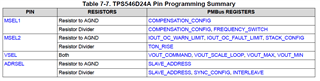
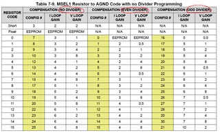
I see a lot of setting is based on resistor code,

 but in the datasheet it doesn't mentioned how to choose divided resistor according to each code.

for example what is 0 mean in resistor code?

would you show me ?

  • Fred, US team will check and give feedback by next Monday.

  •  

    The TPS546D24A uses a 2-stage resistor detection circuit to sense the resistor dividers on the MSEL1, MSEL2, VSEL, and ADRSEL pins.  The conversion from Resistor Codes to the Resistors used appear in the tables 7-17 (R2G Codes 0-7) and 7-18 (R2G Codes 8-15) of the TPS546D24A datasheet. - https://www.ti.com/lit/ds/symlink/tps546d24a.pdf#page=45 

    In the first stage, the resistance from the pin to ground is sensed independent of the top resistor.  This detection circuitry uses the R2G codes:

    Short to Ground, Resistor Values from 4.64kΩ to 82.5kΩ and Open.  The specific resistor for each code is highlighted in Yellow in the second line under the R2G codes across the top.

    In the second stage, the resistor divider ratio is sensed by the voltage on the pin as a fraction of the BP1V5 regulator voltage.  Since the top resistor to achieve the desired ratio is different for each bottom resistor value, the top resistors are listed in a column under the Top Resistor resistance, from Divider Code 0 to Divider Code 15.  Not listed is "Divider Code: None" which does not use the top resistor and instead leaves it open.

    For example, programming the output voltage to 0.92V will use

    divider code 2 (Table 7-12 0.9V to 1.05V in 10mV Steps, use divider code 2) 

    and resistor to ground code 2 (R2G Code = ( 0.92 - 0.90 ) / 0.01 = 2

    In Table 7-17. R2G code 2 uses a bottom resistor of 6.81kΩ and the top resistor for Divider Code 2 with 6.81kΩ bottom resistor is 16.9kΩ

  • Hi James,

    do you know what even divider and odd divider means here?


    they're using 7 TPS546D24 would you help them fill in the right code number?

    especially the current and voltage loop gain. they don't know how to set this thing

    Copy of FG-6500G MB_CPUB_NP7_TPS546D24A setting_Tom 20221128.xlsx

  •  

    do you know what even divider and odd divider means here?

    Even Codes are 0, 2, 4, 6, 8, 10, 12, 14

    Odd Codes are 1, 3, 5, 7, 9, 11, 13, 15

    The LSB of the divider code selects the range of Compensation Codes that are programmed by the Resistor to Ground, allowing 32 compensation codes for each switching frequency.

    Divider Codes 0 and 1 select the same switching frequency, but allow Compensation Codes 0-15 (Divider Code 0) or 16-31 (Divider Code 1)

    There is a Power Stage Design, Compensation, and Pin Programming selection design tool linked in the TPS546D24A product folder that will help guide them to select the correct compensation setting as well as resistors to program it.

    https://www.ti.com/product/TPS546D24A#design-tools-simulation 

  • Hi James,

    my customer calculate the Vloop and Iloop is  3.4 and 4 respectively.

    but we try code 13 and 14, but we just can't find a code that can pass all the spec ( all green).

    any suggestion?

  •  

    To improve the ILOOP / VLOOP ratio, they'll need to increase the current loop gain with either a smaller inductor value and the same ILOOP gain, or a higher inductor value that allows a higher ILOOP gain, or they'll need to add output capacitance, or reduce the ESR to reduce the voltage loop bandwidth.

    Another option would be to increase the switching frequency.  Width the same inductance, a higher switching frequency will allow more loop gain and higher current loop bandwidth, which would, in turn, allow more voltage loop bandwidth.

    It looks like they're still not meeting their transient requirements at Voltage Loop Gain of 4.  The next available pin-strapped voltage loop gain is 8, which is going to require considerably more output capacitance to stabilize and pull the bandwidth down.

    If you are able to share the design spreadsheet you are working with, I might be able to provide some specific values.

  • Hi James,

    see attached, please let us know what you've change.

    beware their they need +-3% ripple +-5% transient spec, please make sure the suggestion cover this spec.

    transient spec: 30% load to 100% load

    TPS546D24A_CPUB 0.9V setting_20221201.xlsx

    thanks

    BTW, they said the output current reported from GUI and the one shown at E-load are different.

    ex. when 0 load, GUI report -5A instead.

  • Fred,

    While some current sense measurement error is expected, especially at near zero load, -5A offset is higher than normal.  I would check their AGND to PGND connection, AVIN to AGND bypass connection and BP1V5 to RTN connection to make sure they are routed correctly.  The Current Sense is sensitive to the AGND to PGND noise, and we've seen some errors when these connections are not routed correctly.

    AVIN's bypass capacitor should be routed to the AGND pin without going through the PGND area under the the exposed pad, which is subject to large switching transients.

    AGND should be directly connected to PGND with a trace under the IC directly between the pad for AGND and the pad for the exposed pad.  It should not be routed through vias into an internal ground plane.

    BP1V5 should be bypassed to DRTN and DRTN should not be connected to any other net other than the ground return for the BP1V5 bypass capacitor.

    For Compensation:

    In order to meet a <45mV output voltage deflection on a 23.8A transient, the output impedance needs to be less than 1.89mΩ.

    The dynamic output impedance of the TPS546D24A converter is CSA  / (VOUT_SCALE_LOOP x VLOOP)

    CSA  for the D24A is 6.155mV/A  (For each phase)

    VOUT_SCALE_LOOP at 0.9V output is 0.5

    You'll need a VLOOP of 8 to meet the transient.

    To Stabilize the loop You'll need enough output capacitance to get the output impedance of the capacitors less 1.53mΩ (6.155mV/A / [0.5 x 8] ) at about 1/8th of the switching frequency.

    At 450kHz, that's going to take about 4x the current output capacitance.  In fact, the design tool is estimating at least 1871μF without ESR and your current design is showing 579μF with the derating on the 330μF capacitor.

    With 450kHz switching frequency and the -35% capacitance derating on the 330μF capacitors, I am seeing you would need at least 6x 330μF + 14x 47μF capacitors to stabilize Code 15.

    If we increase the switching frequency to 650kHz, that requirement drops to 4x 330μF + 8x 47μF using Compensation Code 30.

    In both cases good layout of the output capacitors to minimize parasitic inductance and resistance will be critical.  Output capacitors should be laid out on both sides of the PBC (top and bottom) with the VOUT area between two ground areas and capacitors going to both sides.  Vias from the ground into the ground plane should be placed between the capacitor pads and under the capacitor bodies to reduce loop area and inductance.  It would likely be advantageous to change 2 or even 4 of the 47μF capacitors to 22μF capacitors to spread out their self-resonant frequencies and reduce an impedance peaking.

  • Hi  Peter,

    EVM board usually does good on ground partition

    and they're using this on EVM board, so do you think is there any other cause?

  •  

    Is the cycle by cycle switching period stable?

    What are each of the phases reading?

    Have any of the command parameters other than COMPENSTION_CONFIG been changed?

    Are they reading this with the TI FUSION digital designer GUI?  If so, can they provide screen shots of the Monitor and Configure tabs?  On the Configure Tab, the "Phase Commands" menu will show the current settings for each phase.

  • Hi Peter,

    they're using the GUI at TPS546D24A page at ti.com

    this is  the  screen shot at 0A loading.

  •  

    A -1.7A current sense offset on each of the TPS546D24A converters is within expected tolerances.  It was the -5A offset, one what I believed as a single-phase design based on the previously shared information that appeared to be out side of expected tolerances.

  • Hi Peter,

    sorry, customer wasn't expressing the right message to me, but looks like it's not an issue.

    BTW, you mentioned the layout of cap should be critical. 

    should they be closer to TPS546D24A or the loading?

  •  

    For minimizing ESR/ESL and maximizing the transient performance that can be achieved with a specific output capacitance, the best placement of the Output Capacitors is:

    1) Smallest ceramic capacitors should be split between closest to the inductor output terminal and load, with increasing size/value towards the middle.  Electrolytic capacitors with the highest ESR and largest capacitance values should be placed in the middle.

    2) Capacitors should be mirrored on top and bottom and either side of the VOUT areas.  This creates a virtual "feed-through" layout when viewed from the PCB cross-section with VOUT in the middle and ground on top and bottom of both right and left sides.

    3) VOUT and GND pour spacing should be as narrow as design rules allow

    4) When capacitor bodies are large enough for design rules to allow GND vias under the body of the capacitor, Vias should be placed under the body of the capacitor between the VOUT and GND terminals

    5) Vias should should be spaced far enough to allow pours to route between vias to avoid slotting, this is especially true for vias not connected to GND and GND vias when additional VOUT pours are used.

    6) An uninterrupted GND return to the exposed thermal pad should be provided under the VOUT path on the layer immediately below the VOUT.

    These layout guide-lines will help minimize the parasitic capacitance and inductance from the layout and reduce the loop frequency when the output capacitors ground impedance (Zout) falls below the output impedance of the TPS546D24A controlled converter and ensuring stability.

  • Hi Peter,

    they decided to go with your setting with 650KHz and (4x 330μF + 8x 47μF) at first.

    but they found they can pass their spec with only ( 3x 330μF + 4x 47μF), if they want to keep this way due to area constraint,

    do they need to change anything setting related to compensation?

    BTW, can you help check if the 3.3V power rail have  setting from your point of view?

    please help check if there's a better option for Cout and L and compensation code


    TPS546D24A_CPUB 3.3V setting_20221201.xlsx

  •  

    You didn't say which Compensation Code you were using for this 3.3V rail, but looking over the design, yes it looks like 3x 330μF + 4x 47μF would work with Compensation Code 28 or 31.

    The higher inductance (1.0μF) is limiting the current loop bandwidth, as is the transition between the 330μF capacitors with 9mΩ ESR (54kHz ESR Zero) and the 47μF 2mΩ ESR (1.7MHz ESR Zero) capacitors.  The Inductor and 47μF capacitors is placing a minor lightly damped resonance right where we'd like the loop to crossover, which is likely why they are seeing 2x 330μF + 4x 47μF not passing when the loading current gets high enough.

    If they can switch to a 680nH inductor, it looks like they could use Compensation Code 28 or 29 with 2x 330μF + 4x 47μF and still have a stable system.

  • Hi Peter,

    No, I think you got it wrong , 

    these 650KHz  tests were all 0.9V power rail which you already recommended to use compensation code 30 last week.

    so they're all tested in code 30 and 0.22nH.

    The 3.3V today is the another new power rail, please separate these two in case you mistaken.

    so again,

    1. can they use  3x 330μF + 4x 47μF with same compensation code 30 on 0.9V while you suggest  4x 330μF + 8x 47μF last week?

    2.  and please suggest a suitable setting and L&C for new 3.3V power rail , they're going to have next test tomorrow.

    Copy of TPS546D24A_CPUB 3.3V setting_20221201 (002).xlsx

    3.  about the failed test for 0.9V , noted that they used 0.22uH not 1uH (for 3.3V).   so why with the same total capacitance, 6mohm POSCAP ESR  case can pass but 9mohm can't?

    they need these three answers urgently

    thanks a lot

  •  

    Mixing rails without clearly identifying that you are referring to different rails, and extending resolved threads with new, unrelated questions is creating confusion.  In the future, once a question is resolved, select "this has resolved my issue" and open a new thread for a new question / issue rather than continually using the same thread for new issue after issue.

    1. can they use  3x 330μF + 4x 47μF with same compensation code 30 on 0.9V while you suggest  4x 330μF + 8x 47μF last week?

    Based on the provided capacitor information, I see low margin on the 0.9V rail with 3x 330μF (-35% Derating, 4.5mΩ) + 4x 47μF (-20% derating, 1mΩ ESR)  using Compensation Code 30.  While this is working on 1 unit in the lab under nominal operating conditions, some devices with lower than nominal output capacitance could experience ringing in their recovery.  4x 330μF + 4x 47μF is still marginal, but less so and more likely to work over mass production.

    2.  and please suggest a suitable setting and L&C for new 3.3V power rail , they're going to have next test tomorrow.

    See my prior post.

    3.  about the failed test for 0.9V , noted that they used 0.22uH not 1uH (for 3.3V).   so why with the same total capacitance, 6mohm POSCAP ESR  case can pass but 9mohm can't?

    Higher capacitor ESR increases the output impedance of the output capacitor bank over all frequencies, this increases the voltage loop bandwidth and reduces available phase margin.  This also increases the resonant peaking of the Inductor - Ceramic Capacitor resonance since there is less damping to suppress that resonance.

    You can see this in the design tool.  

    Using the 0.6V converter with Compensation Code 30, 220nH inductor and 3x 330μF + 4x 47μF capacitors.  When the ESR of the 330 capacitors are 4.5mΩ the projected bandwidth is 145kHz with 35.8 degrees of phase margin and 7.7fB of gain margin.  Increasing the ESR to 6mΩ, increases the bandwidth to 159kHz and reduces the gain margin to 6.7dB.  At 9mΩ the projected bandwidth is 189kHz, the phase margin only 26 degrees and the gain margin only 4.5dB

    The increasing ESR increases the total output impedance (Zout), increasing the bandwidth and eroding the stability of the design.

  • Hi Peter,

    sorry, I got you. I've started a new post  for 3.3V issue.

     I hope we can continue this forum on the rest question.

    thanks

    1.   how about 3x 330μF + 8x 47μF for "0.9V" ? is it still acceptable for mass production?

    3. why ESR of POSCAP would affect the resonance of MLCC and inductor, would you elaborate on this ?

    appreciate a lot.

  • 1.   how about 3x 330μF + 8x 47μF for "0.9V" ? is it still acceptable for mass production?

    With Compensation Code 30, Using the -35% derating on the 3x 330μF capacitors provided in the excel tool, this still looks marginal, even with 8 of the 47μF.  It's better than it was with only 4x 47μF.  If they can reduce the voltage loop gain to VLOOP = 4 (Compensation Code 29) and still meet their transient requirements, that would be stable, but I don't see it meeting a 45mV Over/Under shoot spec on a 23.8A transient.

    3. why ESR of POSCAP would affect the resonance of MLCC and inductor, would you elaborate on this ?

    If the Resonance Frequency of the Inductor and MLCC capacitors is above the ESR zero of the larger POSCAP capacitors, the ESR of the of the POSCAP capacitors presents itself as a parallel damping resistor to the resonance of the Inductor and MLCC capacitors.  The lower this damping resistor the more energy it removes from the L-C resonance tank and the more damped that resonance is.

    Increasing the ESR of the POSCAPS impacts the resonance of the Inductor and MLCC capacitors in two ways:

    1) It reduces the ESR zero frequency of the POSCAPS, separating the ESR zero from the resonance

    2) It increases the parallel damping resistance, which reduces the damping effect by reducing the energy the ESR absorbs from each cycle of the resonance.