This thread has been locked.
If you have a related question, please click the "Ask a related question" button in the top right corner. The newly created question will be automatically linked to this question.
Dear Specialists,
My customer is considering UCC27324 and has questions.
I would be grateful if you could advise.
---
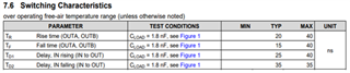
(1) According to the latest data sheet (Rev.J) of UCC27324, the maximum value of TD2 in the switching characteristics is 35ns, but isn't it 50ns?
In Rev.G, it was 50ns.
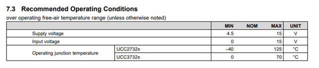
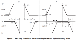
(2)VDD in Figure 1. is 5V, but what is the actual maximum/minimum value, 5V+/-% ?
Or is this 4.5V~15V?
---
I appreciate your great help in advance.
Best regards,
Shinichi
Hi Shinichi,
Our expert for this part is out of office. He can add more inputs when he is back after his vacation.
1. By looking into the latest datasheet, the max TD2 is 35nsec. So you can consider the latest defined max value.
2. VDD pin's operational range is defined in the recommended operating table. Yes, the operational range is between 4.5 to 15V
Thanks
Sasi
Hi Sasi,
Thank you for your reply.
(1)The customer is worried about typo about TD2 maximum value.
Could you please let us know from which revision did it change and background?
(2)I understand the operational voltage range(VDD) is 4.5 to 15V
Regarding test condition, how is the accuracy of 5V, what %?
I'm looking forward to waiting more advise from the expert.
I appreciate your great help and cooperation.
Best regards,
Shinichi
Hi Shinichi,
I am not sure about the history of the spec - we need to wait for the expert to answer that question after his vacation.
On the plot, OUT= 16V and INPUT =5V, per the spec table, the INPUT threshold min is 2V, so INP voltage > 2V will set OUT to high.
Hope it answers your question.
Thanks
Sasi
Hi Sasi,
Thank you for your reply.
Regarding
(1), We' re lookin forward to waiting the answer from the expert.
(2), Please let me know the voltage value of VDD when testing the switching characteristics.
It is 5V in Figure 1 of datasheet.
What is the actual voltage value?
Is it 4.5V?
Or 5V ± what percentage?
I appreciate your great help and cooperation.
Best regards,
Shinichi
Hi Shinichi,
By looking into the following plots, you can observe the TD1 and TD2 values across VDD supply voltages for different gate capacitance. So the spec is supported for the entire VDD operating range of the VDD for 1.8nF Cload.
It also answers that the max TD2 is 35nsec and may not be a typo. Hope it answers your question. I will close the ticket for now.
Please press resolved button if it answers your question.
Thanks
Sasi
Hi Sasi,
Thank you for your reply.
I understand TD1 and TD2 is supported all VDD supply voltage range.
Also, TD2(35ns) is not a typo.
I'll share these information with the customer.
When they have an additional question, I consult you a new thread.
I appreciate your great help and cooperation.
Best regards,
Shinichi