This thread has been locked.

If you have a related question, please click the "Ask a related question" button in the top right corner. The newly created question will be automatically linked to this question.

LM5118: finalisation of design for production

Part Number: LM5118

hi,

i am boulding a powersupply that i can use in multiple applications. the fist one is a stable and protected automotive powersupply for an industrial pc on a trailer.

24V 3A. i have used weebbench power designer to assemble the first prototype. after testing i am pleased i got it to work but am not yet trusting this design i have a few questions.

these are my testresoults please comment on these if this is ''good'' or not:

1: at 1.5A the inductor is already heating up say about 40 degreas celcius. as are all the capacitors (ceramic and electrolytic) in the output circuit. frequency is about 290 Khz what can i do to make the load lighter on the capacitors maybe add more to spread the laod?

2: on my scope i saw that the M2(second fet to ground) is switched on in buck mode Vin:30V at the beginning of the cycle under any load is this normal? why is it? and how does it work?

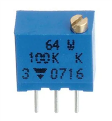
3: i have used slightley different resistors to be in the standard component range. have now an output of about 23.2V give or take. i would like to place a trimming potentiometer. is this advisable? becouse trimming potentiometers have coils of wire inside and im scared that that would couse problems. for examplt the type of POT i would use is added as attatchemtn below. please ignore the value i will use a smaller value.

4: i want to make a 12V output version as well. i can redo the design in webbench power design but is it also possible to change some resistors in the feedback circuit? 

34: what changes are safe to make in the resistors of the feedback circuit. what are the rules? is it a simple resitor voltage devider or does it also influence the circuit to COMP on the LM5118?

5: at testing i also did an output short test and saw that after a few seconds rhe output diode got really hot. output voltage was very low like 0.8V or so and current 7.5A. i will be placing a 3A slow fuse at the output in my final design for the case of an output short circuit. is this normal behaviour or a foult in my design?

6: i placed a TVS diode at the output just in case. this is just from experienses with questionable buckboostconverters that are not soutible for automotive applications. does it still make sense to use it is there any rare case where this protection would be usefull?

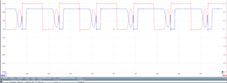
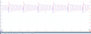
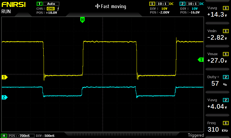
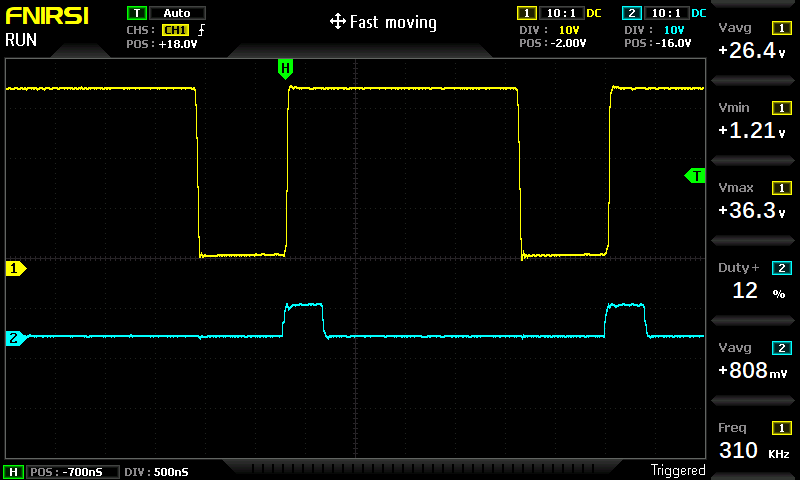
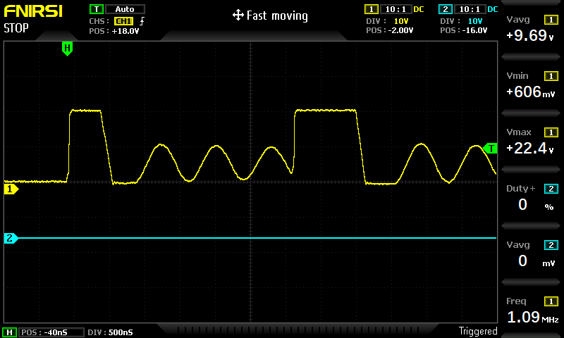
the shots of the ociloscope are both sides of the inductor related to ground. 

Red line is the high side that switches to Vin

vlue line is the low side that is connected to the output diode.

the shot that has perfect square waves is at load of 1.5A

the one with almost completeley sinusoidal waves @1.4 Mhz is no load.

other one is at 1.5A load

all are taken in buck mode at 30V Vin

at the end i want to say that i am very inpressed by the IC and the webbench designer. with little expertise on this subject i was able to bould a buckboostconverter. thank you for making that possible!

 7041.WBDesign18.pdf

  • Hi Michel,

    Thank you for using E2E forums, I am not sure what is the question could you please elaborate on your question?

    Thank you 

    BR,

    Haroon

  • hi,

    thank you for replying to my post.

    i asked multile questions i will try to better describe my questions please see the questions whritten below:

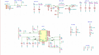
    please use my first post for the puctures of the scopes and circuit.

    1: at 1.5A the inductor is already heating up say about 40 degreas celcius. as are all the capacitors (ceramic and electrolytic) in the output circuit. frequency is about 290 Khz. the powersupply is rated for 3A.

      - will this couse more heat?

      - where does this heat come from? all the devises are rated for this current and frequency.

    2: on my scope i saw that the Q2(second fet to ground) is switched on in buck mode Vin:30V at the beginning of the cycle under any load is this normal? why is it? and how does it work?

       - when i see a standard buck converter there is no FET to ground and it does not need one also. why is this switched on for a moment?

       - i ask this becouse it didnt make any sense to me to switch it on and i am afraight that i might have made a mistake on my board design.

    3&4 the feedback curcuit... resistor devider from VO to FB and GND / the circuit with 2 caps and 1 resistor between FB and COMP.

    - can i simply change the resistor devider circuit with ather resitors to get different output voltages?

    - i ask becouse i want  to make a 12V version as well 

    - i ask becuose i want to place a trimming potentiometer to fineley adjust to exact 24.0V

    5: at testing i also did an output short test and saw that after a few seconds the output diode got really hot. output voltage was very low like 0.8V or so and current 7.5A. i will be placing a 3A slow fuse at the output in my final design for the case of an output short.

    - question is this current limit of about 7.5A is really high for a 3A rated powersupply. can i change this? how?

    6: i placed a TVS diode at the output just in case of a voltage peak. this TVS diode is placed away from the output diode and caps. and starts conducting at about 30V.

    - can this couse problems in the long term say when caps are degrading and not all spikes are captured by the capacitors?

  • hi,

    input voltage range is about 18 to 35V say a battery voltage of a 24V vehicle.

    i placed different resistors at uvlo to switch off at 18V 63K & 4K7 this works well now.

    those aricles are very usefull this will be implemented in the fnal board. and the calculater is a great toll to check my design afterwards.

    i have been doing more tests and found that the output diode was not recovering fast enough. i think i made it too hot by soldering becouse after replacing the heat went down a good bit.

    question 1 is probably the diode i have to do more tests so for now done:)

    question 2 i think it is becouse it is still in buck/boost transient mode at 30V please correct me if i am wrong.

    question 3&4 feedback circuit is easy to fix witht he excel sheet so thats fixed for me

    question 5 current limit is set by the limit resistor i saw in the datasheet could have known without asking.

    question 6 the TVS diode in the output circuit is it safe to use or can it couse problems?

    i have a new question after testing.

    question 7 in boost mode Vin 18V and Iout 1.5A the converter starts but the output voltage never reaches the 24V it is making a noisy high pitch noise. the converter is not 'starting up'. when no load is attatched it starts up easy. with a small load it takes about 1 second to 'start up'. can you give me a clue as to what is going on?

    thanks in advanse

    BR.

    michel datema

  • Hi michel,

    Please add some waveforms for you questions.

  • hello guys,

    i am now just doing more tests but am not learning anything from them. it behaves different than i expect.

     MR Feng JI. what waveforms do you want to see specificley? where do you want me to place the probes? please note that in my first post i put a lot of waveforms with the probes around the inductor.

    with todays tests i placed the probes on the output diode again. i see a lot of spiking the diode is still heating up more and more.

    when the circuit is under no load it easily starts up in boost mode. the freqency is varying a lot from 300 to 900Khz only stabilizing under a load.

    finally while testing i broke of the input electrolytic capacitor at 27.5V by mistake. this fryed the lm5118 ic. 

    i will be replacing it but i am either having the worst of luck or a bad design.

    can anybody explain to me the varying frequency?

    why the chip fries if the input capacitor braks off?

    what i can do check about the spiking at the optput diode or is it normal?

    what can be the couse of the buck startup problem?

  • Hi Michel,

    Please specify the problem you met, we are not able to solve every problem you met when debug.

    Best Regards,

    Feng Ji

  • is it normal for the IC to change the frequency varying from 300 up to 900 khz when there is no load on the output?

    is spiking on the output diode normal? i use 300 khz and BSC123N08NS3G diode

    when a input capacitor braks off the ic goes dead... what can be the reason for this?

  • Hi Michel,

    The frequency will not change from 300kHz to 900kHzwhen there is no load on the output. Do you have waveforms for this issue?

    What does spiking on the output diode mean? BSC123N08NS3G is power MOSFET

    It will be difficult to tell why when a input capacitor braks off the ic goes dead.

    Best Regards,

    Feng Ji

  • hi,

    The frequency will not change from 300kHz to 900kHzwhen there is no load on the output. Do you have waveforms for this issue?

    What does spiking on the output diode mean? BSC123N08NS3G is power MOSFET

    yes i put the wrong part noumber  this is the diode i use: SBRD10200TR

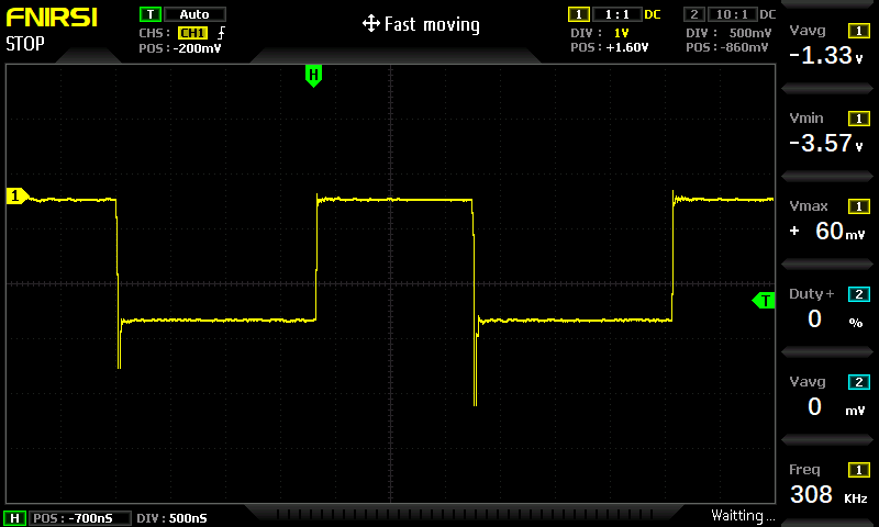
    i made a waveform of the output diode at 1.5A load (50% of the capacity) here the diode is heating up quite a bit. please note the high voltage drop...

    i replace this diode a few times hoping on better resouts but none yet.

    the probe and gnd from the scope were directley on the diode poles

    with the spiking i mean the yellow line under tha wave. it does not happin every wave but some times.

    the startip problem is as follows:

    the devise has to switch on in boost mode due to UVLO. at about 18~19V under no load it switches on instantley and no problems occur.

    when i switch on with a load attatched the devise only switches on at 27 or so volt.

    i will place some scopes: yellow line is the gate of input mosfet // blue is gate of boost mosfet

    boost: VI20V

    buck:VI30V

    startup problem:

    please tell me your opinion how can i change this startup problem?

    should i find another output diode? 

  • Hi Michel,

    can you share your layout - i would like to check and ensure that the issues you have described are not generated due to layout issues.

    Thanks,

     Stefan

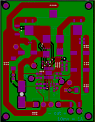
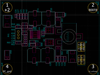
  • hi this is the layout of this test board.

    i placed a lot of components apart to be able to reach them easily.

    in the mean time i learned a lot about the layout also the official version will be mutch different.

    please comment on it:)

    8540.schematic.pdf

  • HI Michel,

    i see several issues in the layout which might trigger the issues you have observed:

    - the Current sense (R2) should be connected to CS and CSG with a Kelvin connection (dedicated wires, both routed in parallel with a very low area in-between)

    - the AGND should be connected via the Thermal pad to the common GND

    - All AGND related components should be connected as close as possible to the AGND pin e.g.  RT (R9) has a very large ground loop a

    - Vcc can GND connection would be better to directly connect to PGND

    To the scope plots above:

    Plot 1 (Spiking): why do you have a negative pulse here? The spikes are from parasitic of the circuit - most come from layout and reverse recover charge of the Diode

    Startup problem - might be related to the to high sense resistor as mentioned above - the device might detect an over current as beside the normal load also the charging of the output caps needs to be done.

    Last plot: this is the typical waveform when the SMPS operates in DCM (which could be the case with no or low load)

    Can you be more specific on this point and add some scope plots showing that : frequency changes from 300khZ to 900kHz

    Best regards,

     Stefan

  • hi stefan

    - the Current sense (R2) should be connected to CS and CSG with a Kelvin connection (dedicated wires, both routed in parallel with a very low area in-between)

    i placed the wire but i did not see the cupper poore pooring over it thats my mistake can my tests still be relyable? or should i place 2 seperate wires to test this.

    - All AGND related components should be connected as close as possible to the AGND pin e.g.  RT (R9) has a very large ground loop a

    i made the notes for the final board thanks does it make test unrelyable?

    Plot 1 (Spiking): why do you have a negative pulse here? The spikes are from parasitic of the circuit - most come from layout and reverse recover charge of the Diode

    do you think the forward voltage is high on this? datasheet sas 0.7V this seems to be more. the diode is getting hot under 1.5A output load. do you think this is normal?

    Startup problem - might be related to the to high sense resistor as mentioned above - the device might detect an over current as beside the normal load also the charging of the output caps needs to be done.

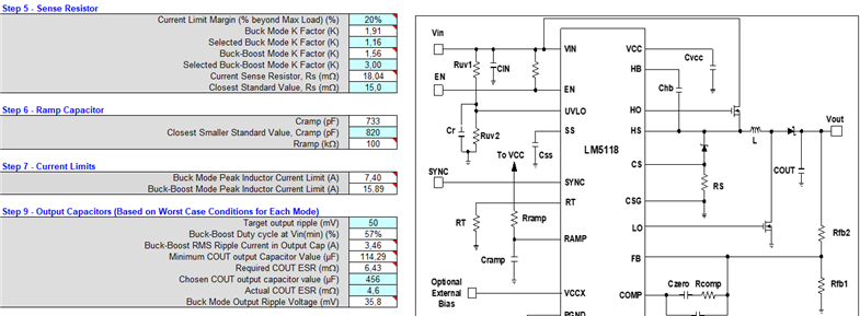
    i can do a test with a 0.01Ohm or 0.005Ohm both available. i was playing with the excel sheet and found this out:

    buck 7.4A // boost 15.89A isnt that already really high? 

    Last plot: this is the typical waveform when the SMPS operates in DCM (which could be the case with no or low load)

    i see 1.09Mhz really high. it makes a high pitch noise in this mode.

    the load is here 1.5A@24V only the output voltage of 24V is not reatched.

    the noise scares me a little all parts are heating up in this mode that not working in DCM mode

    input voltage is here above 18V and under 26V 

    this is the last scope plot in my previous post

    Can you be more specific on this point and add some scope plots showing that : frequency changes from 300khZ to 900kHz

    i think you already anwered this can this be the DCM mode? or am i just reading the scope wrong in this case? its regarding the 1Mhz at the last picture of previous post

  • stefan.

    i just checked my sense resistor it was a 0.005Ohm resistor

    i placed the 0.015 per webbench designer and the area where the converter would not start went from 19.0 to 19.3V

    with a 0.01 Ohm resitor there is no problem at all!

    is it safe for me to sticke with the 0.01Ohm sense resistor?

  • Hi Michel,

    is this right that you first had 5mOhm in - just wanted to ensure as this looks strange.

    To check if the 10mOhm is save you need to check on the peak current limit you get then, with 10mOhm this gives

    14.7A in Buck

    30.0 A in Boost

    So you need to check your circuit if this is able to handle this current, esp,

    - MOSFET

    - Inductor (I DC and I saturation)

    - shunt power rating

    Best regards,

     Stefan

  • hi stefan

    thank you for replying. this is what i gound:

    the mosfet can handle 55A so that works

    about the inductor i dont really understand whats going on there can you teach me how to read this?

    https://www.we-online.com/components/products/datasheet/7443632200.pdf <- datasheet :)

    i can not understand how an inductor of this size would not fit into a small 3A buckboost converter 

    Shunt is 3W 10mVx30A is 0.3W this is more than good enough.

    BR.

    michel

  • Hi Michel,

    The MSOFET will be OK.

    Also for the inductor you should not seen any issue for normal operation, here the max inductor current  and also the RMS current will stay below 4.5A. So you should not have an issue with the selected inductor.

    The current limit given in Step7 of the Excel sheet are representing the max current just limited by the shunt and over current protection.

    So in a failure cause (short at the output) you can reach that current before the controller detects it and shut off. 

    In this case the inductor can already go into saturation or gets overloaded due to the to high current.

    I am not sure for which sense resistor the above screenshot of the Excel quickstart calculator was done, but you may can check again.

    Best regards,

     Stefan

  • Hi guys.

    It looks like it has been fixed. I had the problem of the diodes heating up fast. They were bad i think. I tryed to find another diode thats a good replacement and found the pds760-13 had a lower voltage drop but the spiking is gone so i think that solved the problem. After that i placed the 15mohm shunt back and there was also no startup problems any more. Also it is using 3W less from the power supply now under the same load.

    It is time for long period testing so see it it will be robust enough.

    I will ofcourse update you on the resoults but for now i am already very happy with the resoults 

  • Hi Michel,

    thanks a lot for the update.

    I have not seen an update for the last 12 days, so I assume the questions are/or answered and the issue is solved.
    I close this thread now. If there is still something open reply and the thread will get open again.
    If you have any other question or of the thread gets locked, please open a new one.

    Clicking the Resolved Button also helps us to maintain this forum.

    Best regards,
    Stefan

  • hi stefan,

    yes it looks like everything is clear for me now.

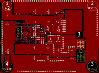
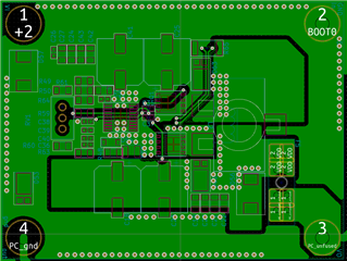
    im now working on the final board. this is my newest design please feel free is you see any foults