This thread has been locked.

If you have a related question, please click the "Ask a related question" button in the top right corner. The newly created question will be automatically linked to this question.

BQ40Z50-R1: How to enable Temperature protection in fuel gauge

Part Number: BQ40Z50-R1
Other Parts Discussed in Thread: BQ40Z50, BQSTUDIO, BQ40Z50-R2

Hi All,

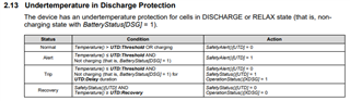
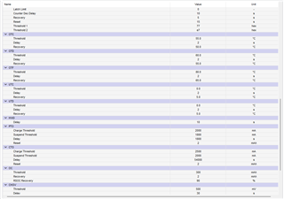
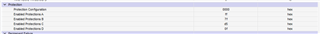
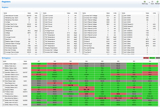
I am trying to enable over temperature and under temperature protection on BQ40Z50 fuel gauge. I tried to write temperature value into cell temperature hopping that setting high value for temperature will over automatically enable the protection by reducing charging or discharging current or by disabling the pass FEs. I was able to manually write high temperature values to FG by writing to Sbs_Configuration and set SMB-CELL_TEMP bit to 1. I was able to see the change in BQStudio as well. but there was any protection mechanism enabled by this high temperature. While reading through the reference manual it was understood that there are some registers i need to set and some other operations are needed. I need help in understanding this. Below are my queries.

1) What are the operations i need to do in fuel gauge to enable temperature protection.

2) What are the protections that i can enable in the fuel gauge related to temperature.

3) How does this protection mechanism works.

It will be great if i could get this questions answered. 

Thanks,

PG

  • Hello PG,

    The TRM has a good description of how protections work. See Chapter 2 https://www.ti.com/lit/ug/sluubc1d/sluubc1d.pdf

    Section 2.8 deals with temperature. The selection of thermistors needs to be configured. DA configuration needs to be updated. I don't think cell temperature can be written on bq40z50 as it seems to be marked as a read only register.

  • Hi,

    It is mentioned that the write_temp is a write only register and it is 16 bit. The resolution is .1 K. I can see this working as well. Also when i read getting  "0x08 Temperature()" register,  I am able to read back the value i am writing to write_temp register. In my use case i am disabling thermistors  by writing to Sbs_Configuration and set SMB-CELL_TEMP bit to 1. Below image i am writing 50 deg C and it is reflecting in BQstudio.


  • Have one more doubt, is the cell temperature used as an input to temperature protection, because for the current project I am working on i wont be relaying on NTC as temperature data source, but we will write temperature values to cell temperature and see the effect of temperature on the system. 

  • Hello Priyan,

    The protection section does not reference host written temperature configuration, therefore it is possible that it is not a valid configuration for protection to  get triggered. I will assign this thread to Wyatt since he helped you with the write_temp earlier.

  • Hello Priyan,

    Can you share the .gg file for your gauge configuration as well as a BQStudio log of the test you are trying to do? If you do not have the protections enabled then even if you set the temperature high nothing will happen.

    Sincerely,

    Wyatt Keller

  • Hi Keller,

    I have not enabled the protection feature. I am trying to understand how and what i need to do to enable this. Basic input will help me start with the enabling process. I have gone through the user manual and it was bit hard for me to understand. Can you give me a basic brief of what i need to do to enable the protection, while charging and discharging. I will share the log and .gg file tomorrow.

    Thanks.

    PG

  • Hello Priyan,

    You should be able to set all the protection in BQStudio under data memory->settings there is a section for protections and PF.

    Sincerely,

    Wyatt Keller

  • Hi Keller,

    I have few more follow up questions related to this. Our use of fuel gauge is different compred to conventional battery. We are using this fuelguage to develop a battery simulator where we can change temperature and voltage to mimic real battery sinarios. As such we are using write_temp command to directly write the cell temperature without using sensors. Following are my questions.

    1) Using only Cell temperature data, can we enable temperature protection.

    2) Can we use the cell temperature for over and under temperature FET protection, over and under temperature protection for charging and discharging and so on.

    3) What are all the temperature protection i can enable by writing cell temperature if all are not possible.

    Thanks,

    PG

  • Hello Priyan,

    I would not recommend setting up a battery simulator for the gauge, the algorithm is quite complex and you will probably run into multiple issues depending on what type of tests you plan to run. The best way to run gauge testing is with a real battery and a battery cycler like Arbin or Maccor along with a temperature chamber.

    You should be able to configure the USER_TS so that it is set for the Cell Temperature and should trigger protections.

    Sincerely,

    Wyatt Keller

  • Hi Keller,

    In the current design we have implemented, the board doesn't have NTC on it. The host is sending the temperature value to the FG and it is written to the cell temp register through write_temp command. This is working as we are able to see the change in BQStudio. We would like to know following.

    1) In this method too will we be able enable enable temperature protection?

    2) If possible, which are the registers we need to enable. Current code we are increasing the temperature above 200deg C and we are not seeing any protection kicking in.

    3) What are the expected behavior during under/over temperature situations with respect to the settings we need to enable in FG registers.

    4) "You should be able to configure the USER_TS so that it is set for the Cell Temperature and should trigger protections.". Is this USER_TS any register in FG because we are not able to locate this in user manual.

    Thank and regards,

    Priyan George

  • Hello Priyan,

    let me look into this further, I need to check with the firmware team if the temperature supplied by user can be used for protections.

    sincerely,

    Wyatt Keller

  • Hi Keller,

    Please check and update the same so that we can have this implemented in our design. As per the understanding from user manual, it has to support I believe. Awaiting your confirmation.

    Thanks,

    Priyan George

  • Hello Priyan,

    Waiting for their feedback now.

    Sincerely,

    Wyatt Keller

  • Hello Priyan,

    Feedback was that the firmware uses the user input for the temperature just like the ADC input that the gauge would normally measure. So you must configure the settings to trip.

    Sincerely,

    Wyatt Keller

  • Hi Keller,

    Just to clear my doubt, is there any specific register we have to configure to enable the protection if we implement in this method.

    Or  can you give me the list of registers that i have to configure to get this working. Currently we are not able to  see any change in behavior when we write high temperature to the FG although the temperature value is set correctly and we are able to read back the same in BQstudio.

    Thanks and regards,

    Priyan George

  • Hello Priyan,

    Yes all the conditions outlined in the TRM for the temperature protections. For example, UTD all of these condition must be met:

    You must also make sure the actual protection is enabled in the Settings section of data memory, it should be enabled by default.

    Sincerely,

    Wyatt Keller

  • Hi Keller,

    Following are the settings done for temperature the FG.

    Following are the protection enabled.

    Following image captures the cell temperature and the mosfet states. it is observed that at 99deg C both the mosfets are still on even though my temperature settings are well below this temperature. This is same in case of charging and discharging.

    Are we missing anything here. Please help.

    Thanks and regards,

    Priyan George

  • Hello Priyan,

    The FETs are still on because you are in the FET test mode and have manually turned them on. The gauge will not control the FETs when you have FET_EN = 0. FET_EN must be set to 1 for the gauge to control the FET action.

    Also you must have the correct TempEn set. Please share your .gg file and log of tests.

    Sincerely,

    Wyatt Keller

  • Hi Keller,

    As i was unable to attach the .gg file, pasting it here for your reference.

    Thanks,

    Priyan George

    * Texas Instruments Data Flash File
    * File created Tue Feb 14 15:38:55 2023
    *
    * Device Number 4500
    * Firmware Version 3.09
    * Build Number 73
    * Order Number 0
    *
    * bqz Device Number 4500
    * bqz Firmware Version 3.09
    * bqz Build Number 73
    *
    * Field Order: Class name  Subclass name  Parameter name  Parameter Value  Display Units
    Calibration Voltage Cell Gain 12101 -
    Calibration Voltage Pack Gain 49669 -
    Calibration Voltage BAT Gain 48936 -
    Calibration Current CC Gain 0.966 mOhm
    Calibration Current Capacity Gain 0.966 mOhm
    Calibration Current Offset CC Offset 0 -
    Calibration Current Offset Coulomb Counter Offset Samples 64 -
    Calibration Current Offset Board Offset 0 -
    Calibration Current Offset CC Auto Config 3 hex
    Calibration Current Offset CC Auto Offset 0 -
    Calibration Temperature Internal Temp Offset 0 °C
    Calibration Temperature External1 Temp Offset 0 °C
    Calibration Temperature External2 Temp Offset 0 °C
    Calibration Temperature External3 Temp Offset 0 °C
    Calibration Temperature External4 Temp Offset 0 °C
    Calibration Internal Temp Model Int Gain -12143 -
    Calibration Internal Temp Model Int base offset 6232 -
    Calibration Internal Temp Model Int Minimum AD 0 -
    Calibration Internal Temp Model Int Maximum Temp 6232 0.1°K
    Calibration Cell Temperature Model Coeff a1 -11130 -
    Calibration Cell Temperature Model Coeff a2 19142 -
    Calibration Cell Temperature Model Coeff a3 -19262 -
    Calibration Cell Temperature Model Coeff a4 28203 -
    Calibration Cell Temperature Model Coeff a5 892 -
    Calibration Cell Temperature Model Coeff b1 328 -
    Calibration Cell Temperature Model Coeff b2 -605 -
    Calibration Cell Temperature Model Coeff b3 -2443 -
    Calibration Cell Temperature Model Coeff b4 4696 -
    Calibration Cell Temperature Model Rc0 11703 -
    Calibration Cell Temperature Model Adc0 11703 -
    Calibration Cell Temperature Model Rpad 0 -
    Calibration Cell Temperature Model Rint 0 -
    Calibration Fet Temperature Model Coeff a1 -11130 -
    Calibration Fet Temperature Model Coeff a2 19142 -
    Calibration Fet Temperature Model Coeff a3 -19262 -
    Calibration Fet Temperature Model Coeff a4 28203 -
    Calibration Fet Temperature Model Coeff a5 892 -
    Calibration Fet Temperature Model Coeff b1 328 -
    Calibration Fet Temperature Model Coeff b2 -605 -
    Calibration Fet Temperature Model Coeff b3 -2443 -
    Calibration Fet Temperature Model Coeff b4 4696 -
    Calibration Fet Temperature Model Rc0 11703 -
    Calibration Fet Temperature Model Adc0 11703 -
    Calibration Fet Temperature Model Rpad 0 -
    Calibration Fet Temperature Model Rint 0 -
    Calibration Current Deadband Deadband 3 mA
    Calibration Current Deadband Coulomb Counter Deadband 9 116nV
    Calibration Interconnect Resistance Cell 1 0 mOhm
    Calibration Interconnect Resistance Cell 2 0 mOhm
    Calibration Interconnect Resistance Cell 3 0 mOhm
    Calibration Interconnect Resistance Cell 4 0 mOhm
    Settings Configuration Charging Configuration 0 hex
    Settings Configuration FET Options 0 hex
    Settings Configuration Sbs Gauging Configuration 0 hex
    Settings Configuration Sbs Configuration 60 hex
    Settings Configuration Auth Config 0 hex
    Settings Configuration Power Config 0 hex
    Settings Configuration IO Config 0 hex
    Settings Configuration GPIO Sealed Access Config 0 hex
    Settings Configuration Flag Map Set Up 1 0 hex
    Settings Configuration Flag Map Set Up 2 0 hex
    Settings Configuration Flag Map Set Up 3 0 hex
    Settings Configuration Flag Map Set Up 4 0 hex
    Settings Configuration LED Configuration 00d0 hex
    Settings Configuration Temperature Enable 6 hex
    Settings Configuration Temperature Mode 4 hex
    Settings Configuration DA Configuration 2 hex
    Settings Configuration SOC Flag Config A 0c8c hex
    Settings Configuration SOC Flag Config B 008c hex
    Settings Configuration Balancing Configuration 1 hex
    Settings Configuration IT Gauging Configuration d0fe hex
    Settings Configuration IT Gauging Ext 001a hex
    Settings Configuration Elevated Degrade Configuration 15 hex
    Settings Fuse PF Fuse A 0 hex
    Settings Fuse PF Fuse B 0 hex
    Settings Fuse PF Fuse C 0 hex
    Settings Fuse PF Fuse D 0 hex
    Settings Fuse Min Blow Fuse Voltage 3500 mV
    Settings Fuse Fuse Blow Timeout 30 s
    Settings Fuse GPIO Timeout 30 s
    Settings BTP Init Discharge Set 150 mAh
    Settings BTP Init Charge Set 175 mAh
    Settings SMBus Address 16 -
    Settings SMBus Address Check ea -
    Settings Lifetimes Lifetimes Configuration 0 hex
    Settings Lifetimes Time RSOC Threshold A 95 %
    Settings Lifetimes Time RSOC Threshold B 90 %
    Settings Lifetimes Time RSOC Threshold C 80 %
    Settings Lifetimes Time RSOC Threshold D 50 %
    Settings Lifetimes Time RSOC Threshold E 20 %
    Settings Lifetimes Time RSOC Threshold F 10 %
    Settings Lifetimes Time RSOC Threshold G 5 %
    Settings Protection Protection Configuration 0 hex
    Settings Protection Enabled Protections A ff hex
    Settings Protection Enabled Protections B 7f hex
    Settings Protection Enabled Protections C d5 hex
    Settings Protection Enabled Protections D 0f hex
    Settings Permanent Failure Enabled PF A 0 hex
    Settings Permanent Failure Enabled PF B 0 hex
    Settings Permanent Failure Enabled PF C 0 hex
    Settings Permanent Failure Enabled PF D 0 hex
    Settings AFE AFE Protection Control 70 hex
    Settings AFE ZVCHG Exit Threshold 2200 mV
    Settings Manufacturing Mfg Status init 8 hex
    Settings Accumulated Charge Accum Discharge Threshold -1000 mAh
    Settings Accumulated Charge Accum Charge Threshold 1000 mAh
    Advanced Charge Algorithm Temperature Ranges T1 Temp 0 °C
    Advanced Charge Algorithm Temperature Ranges T2 Temp 12 °C
    Advanced Charge Algorithm Temperature Ranges T5 Temp 20 °C
    Advanced Charge Algorithm Temperature Ranges T6 Temp 25 °C
    Advanced Charge Algorithm Temperature Ranges T3 Temp 30 °C
    Advanced Charge Algorithm Temperature Ranges T4 Temp 55 °C
    Advanced Charge Algorithm Temperature Ranges Hysteresis Temp 1 °C
    Advanced Charge Algorithm Low Temp Charging Current Low 132 mA
    Advanced Charge Algorithm Low Temp Charging Current Med 352 mA
    Advanced Charge Algorithm Low Temp Charging Current High 264 mA
    Advanced Charge Algorithm Low Temp Charging Voltage 4000 mV
    Advanced Charge Algorithm Standard Temp Low Charging Current Low 1980 mA
    Advanced Charge Algorithm Standard Temp Low Charging Current Med 4004 mA
    Advanced Charge Algorithm Standard Temp Low Charging Current High 2992 mA
    Advanced Charge Algorithm Standard Temp Low Charging Voltage 4200 mV
    Advanced Charge Algorithm Standard Temp High Charging Current Low 1980 mA
    Advanced Charge Algorithm Standard Temp High Charging Current Med 4004 mA
    Advanced Charge Algorithm Standard Temp High Charging Current High 2992 mA
    Advanced Charge Algorithm Standard Temp High Charging Voltage 4200 mV
    Advanced Charge Algorithm High Temp Charging Current Low 1012 mA
    Advanced Charge Algorithm High Temp Charging Current Med 1980 mA
    Advanced Charge Algorithm High Temp Charging Current High 1496 mA
    Advanced Charge Algorithm High Temp Charging Voltage 4000 mV
    Advanced Charge Algorithm Rec Temp Charging Current Low 2508 mA
    Advanced Charge Algorithm Rec Temp Charging Current Med 4488 mA
    Advanced Charge Algorithm Rec Temp Charging Current High 3520 mA
    Advanced Charge Algorithm Rec Temp Charging Voltage 4100 mV
    Advanced Charge Algorithm Pre-Charging Current 88 mA
    Advanced Charge Algorithm Maintenance Charging Current 44 mA
    Advanced Charge Algorithm Voltage Range Precharge Start Voltage 2500 mV
    Advanced Charge Algorithm Voltage Range Charging Voltage Low 2900 mV
    Advanced Charge Algorithm Voltage Range Charging Voltage Med 3600 mV
    Advanced Charge Algorithm Voltage Range Charging Voltage High 4000 mV
    Advanced Charge Algorithm Voltage Range Charging Voltage Hysteresis 0 mV
    Advanced Charge Algorithm SoC Range Charging SoC Med 50 %
    Advanced Charge Algorithm SoC Range Charging SoC High 75 %
    Advanced Charge Algorithm SoC Range Charging SoC Hysteresis 1 %
    Advanced Charge Algorithm Degrade Mode 1 Cycle Threshold 50 -
    Advanced Charge Algorithm Degrade Mode 1 SOH Threshold 95 %
    Advanced Charge Algorithm Degrade Mode 1 Runtime Threshold 8760 h
    Advanced Charge Algorithm Degrade Mode 1 Voltage Degradation 10 mV
    Advanced Charge Algorithm Degrade Mode 1 Current Degradation 10 %
    Advanced Charge Algorithm Degrade Mode 2 Cycle Threshold 150 -
    Advanced Charge Algorithm Degrade Mode 2 SOH Threshold 80 %
    Advanced Charge Algorithm Degrade Mode 2 Runtime Threshold 17520 h
    Advanced Charge Algorithm Degrade Mode 2 Voltage Degradation 40 mV
    Advanced Charge Algorithm Degrade Mode 2 Current Degradation 20 %
    Advanced Charge Algorithm Degrade Mode 3 Cycle Threshold 350 -
    Advanced Charge Algorithm Degrade Mode 3 SOH Threshold 60 %
    Advanced Charge Algorithm Degrade Mode 3 Runtime Threshold 26280 h
    Advanced Charge Algorithm Degrade Mode 3 Voltage Degradation 70 mV
    Advanced Charge Algorithm Degrade Mode 3 Current Degradation 40 %
    Advanced Charge Algorithm Degrade Mode Cycle Count Start Runtime 1 -
    Advanced Charge Algorithm Degrade Mode Runtime Update Interval 10 h
    Advanced Charge Algorithm Degrade Mode Runtime Degrade 0 hours
    Advanced Charge Algorithm CS Degrade Temperature Threshold 50 °C
    Advanced Charge Algorithm CS Degrade Voltage Threshold 4200 mV
    Advanced Charge Algorithm CS Degrade Time Interval 300 s
    Advanced Charge Algorithm CS Degrade Delta Voltage 25 mV
    Advanced Charge Algorithm CS Degrade Min CV 3000 mV
    Advanced Charge Algorithm Termination Config Charge Term Taper Current 250 mA
    Advanced Charge Algorithm Termination Config Charge Term Voltage Offset 75 mV
    Advanced Charge Algorithm Termination Config Charge Term Charging Voltage 4200 mV
    Advanced Charge Algorithm Charging Rate of Change Current Rate 1 steps
    Advanced Charge Algorithm Charging Rate of Change Voltage Rate 1 steps
    Advanced Charge Algorithm Charge Loss Compensation CCC Current Threshold 3520 mA
    Advanced Charge Algorithm Charge Loss Compensation CCC Voltage Threshold 4200 mV
    Advanced Charge Algorithm IR Correction Averaging Interval 12 s
    Advanced Charge Algorithm Cell Balancing Config Bal Time/mAh Cell 1 367 s/mAh
    Advanced Charge Algorithm Cell Balancing Config Bal Time/mAh Cell 2-4 514 s/mAh
    Advanced Charge Algorithm Cell Balancing Config Min Start Balance Delta 3 mV
    Advanced Charge Algorithm Cell Balancing Config Relax Balance Interval 18000 s
    Advanced Charge Algorithm Cell Balancing Config Min Rsoc for Balancing 80 %
    Advanced Charge Algorithm Cell Balancing Config Start Rsoc for Bal in Sleep 95 %
    Advanced Charge Algorithm Cell Balancing Config End Rsoc for Bal in Sleep 60 %
    Advanced Charge Algorithm Cell Balancing Config Start Time for Bal in Sleep 100 hrs
    Advanced Charge Algorithm Elevated Degrade ERM Reset RSoC Threshold 85 %
    Advanced Charge Algorithm Elevated Degrade ERM Reset Voltage Threshold 3700 mV
    Advanced Charge Algorithm Elevated Degrade ERM RSoC Threshold 90 %
    Advanced Charge Algorithm Elevated Degrade ERM Voltage Threshold 4000 mV
    Advanced Charge Algorithm Elevated Degrade ERM Time Threshold 10000 hours
    Advanced Charge Algorithm Elevated Degrade ERETM RSoC Threshold 90 %
    Advanced Charge Algorithm Elevated Degrade ERETM Voltage Threshold 4200 mV
    Advanced Charge Algorithm Elevated Degrade ERETM Temperature Threshold 39.1 °C
    Advanced Charge Algorithm Elevated Degrade ERETM Temperature Max Threshold 49.1 °C
    Advanced Charge Algorithm Elevated Degrade ERETM Time Threshold 10000 hours
    Advanced Charge Algorithm Elevated Degrade ERETM Charging Voltage 3900 mV
    Advanced Charge Algorithm Elevated Degrade Accumulated ERM Time 0 hours
    Advanced Charge Algorithm Elevated Degrade Accumulated ERETM Time 0 hours
    Advanced Charge Algorithm Elevated Degrade ERETM Status 3 -
    Power Power Valid Update Voltage 3500 mV
    Power Shutdown Shutdown Voltage 1750 mV
    Power Shutdown Shutdown Time 10 s
    Power Shutdown IO Shutdown Delay 1 250ms
    Power Shutdown IO Shutdown Timeout 8 250ms
    Power Shutdown PF Shutdown Voltage 1750 mV
    Power Shutdown PF Shutdown Time 10 s
    Power Shutdown PS Shutdown Voltage 2500 mV
    Power Shutdown PS NoLoadResCap Threshold 0 mAh
    Power Shutdown Charger Present Threshold 3000 mV
    Power Sleep Sleep Current 10 mA
    Power Sleep Bus Timeout 5 s
    Power Sleep Voltage Time 5 s
    Power Sleep Current Time 20 s
    Power Sleep Wake Comparator 0 hex
    Power Ship FET Off Time 10 s
    Power Ship Delay 20 s
    Power Ship Auto Ship Time 1440 min
    Power Power Off Timeout 30 min
    Power Manual FET Control MFC Delay 60 0.25s
    Power IATA IATA Config 3 -
    Power IATA IATA Delay Time 10 s
    Power IATA IATA RSOC Threshold 30 %
    Power IATA IATA DeltaV Threshold 50 mV
    Power IATA IATA Delta RSOC 3 %
    Power IATA IATA Wake AbsRsoc 10 %
    Power IATA IATA Min Temperature 10 °C
    Power IATA IATA Max Temperature 40 °C
    Power IATA IATA Min Voltage 3000 mV
    Power IATA IATA Max Voltage 4350 mV
    Power IATA STORE IATA RM mAh 0 mAh
    Power IATA STORE IATA RM cWh 0 cWh
    Power IATA STORE IATA FCC mAh 0 mAh
    Power IATA STORE IATA FCC cWh 0 cWh
    Power IATA STORE IATA Flag 0 -
    Power Unintended Wakeup Delay 2 s
    Power Unintended Wakeup Count 3 -
    LED Support LED Config LED Flash Period 512 488us
    LED Support LED Config LED Blink Period 1024 488us
    LED Support LED Config LED Delay 100 488us
    LED Support LED Config LED Hold Time 4 s
    LED Support LED Config LED FC Time 60 mins
    LED Support LED Config CHG Flash Alarm 10 %
    LED Support LED Config CHG Thresh 1 0 %
    LED Support LED Config CHG Thresh 2 20 %
    LED Support LED Config CHG Thresh 3 40 %
    LED Support LED Config CHG Thresh 4 60 %
    LED Support LED Config CHG Thresh 5 80 %
    LED Support LED Config DSG Flash Alarm 10 %
    LED Support LED Config DSG Thresh 1 0 %
    LED Support LED Config DSG Thresh 2 20 %
    LED Support LED Config DSG Thresh 3 40 %
    LED Support LED Config DSG Thresh 4 60 %
    LED Support LED Config DSG Thresh 5 80 %
    System Data Manufacturer Data Manufacturer Info A Length 32 -
    System Data Manufacturer Data Manufacturer Info Block A01 61 Hex
    System Data Manufacturer Data Manufacturer Info Block A02 62 Hex
    System Data Manufacturer Data Manufacturer Info Block A03 63 Hex
    System Data Manufacturer Data Manufacturer Info Block A04 64 Hex
    System Data Manufacturer Data Manufacturer Info Block A05 65 Hex
    System Data Manufacturer Data Manufacturer Info Block A06 66 Hex
    System Data Manufacturer Data Manufacturer Info Block A07 67 Hex
    System Data Manufacturer Data Manufacturer Info Block A08 68 Hex
    System Data Manufacturer Data Manufacturer Info Block A09 69 Hex
    System Data Manufacturer Data Manufacturer Info Block A10 6a Hex
    System Data Manufacturer Data Manufacturer Info Block A11 6b Hex
    System Data Manufacturer Data Manufacturer Info Block A12 6c Hex
    System Data Manufacturer Data Manufacturer Info Block A13 6d Hex
    System Data Manufacturer Data Manufacturer Info Block A14 6e Hex
    System Data Manufacturer Data Manufacturer Info Block A15 6f Hex
    System Data Manufacturer Data Manufacturer Info Block A16 70 Hex
    System Data Manufacturer Data Manufacturer Info Block A17 71 Hex
    System Data Manufacturer Data Manufacturer Info Block A18 72 Hex
    System Data Manufacturer Data Manufacturer Info Block A19 73 Hex
    System Data Manufacturer Data Manufacturer Info Block A20 74 Hex
    System Data Manufacturer Data Manufacturer Info Block A21 75 Hex
    System Data Manufacturer Data Manufacturer Info Block A22 76 Hex
    System Data Manufacturer Data Manufacturer Info Block A23 77 Hex
    System Data Manufacturer Data Manufacturer Info Block A24 7a Hex
    System Data Manufacturer Data Manufacturer Info Block A25 78 Hex
    System Data Manufacturer Data Manufacturer Info Block A26 79 Hex
    System Data Manufacturer Data Manufacturer Info Block A27 30 Hex
    System Data Manufacturer Data Manufacturer Info Block A28 31 Hex
    System Data Manufacturer Data Manufacturer Info Block A29 32 Hex
    System Data Manufacturer Data Manufacturer Info Block A30 33 Hex
    System Data Manufacturer Data Manufacturer Info Block A31 34 Hex
    System Data Manufacturer Data Manufacturer Info Block A32 35 Hex
    System Data Manufacturer Info B Manufacturer Info Block B01 1 Hex
    System Data Manufacturer Info B Manufacturer Info Block B02 23 Hex
    System Data Manufacturer Info B Manufacturer Info Block B03 45 Hex
    System Data Manufacturer Info B Manufacturer Info Block B04 67 Hex
    System Data Integrity Static DF Signature 0 hex
    System Data Integrity Static Chem DF Signature 73b5 hex
    System Data Integrity All DF Signature 0 hex
    SBS Configuration Data Remaining AH Cap. Alarm 300 mAh
    SBS Configuration Data Remaining WH Cap. Alarm 432 cWh
    SBS Configuration Data Remaining Time Alarm 10 min
    SBS Configuration Data Initial Battery Mode 81 hex
    SBS Configuration Data Specification Information 31 hex
    SBS Configuration Data Manufacture Date 1/1/1980 date
    SBS Configuration Data Serial Number 1 hex
    SBS Configuration Data Manufacturer Name Texas Instruments -
    SBS Configuration Data Device Name bq40z50-R2 -
    SBS Configuration Data Device Chemistry LION -
    Lifetimes Voltage Cell 1 Max Voltage 0 mV
    Lifetimes Voltage Cell 2 Max Voltage 0 mV
    Lifetimes Voltage Cell 3 Max Voltage 0 mV
    Lifetimes Voltage Cell 4 Max Voltage 0 mV
    Lifetimes Voltage Cell 1 Min Voltage 32767 mV
    Lifetimes Voltage Cell 2 Min Voltage 32767 mV
    Lifetimes Voltage Cell 3 Min Voltage 32767 mV
    Lifetimes Voltage Cell 4 Min Voltage 32767 mV
    Lifetimes Voltage Max Delta Cell Voltage 0 mV
    Lifetimes Current Max Charge Current 0 mA
    Lifetimes Current Max Discharge Current 0 mA
    Lifetimes Current Max Avg Dsg Current 0 mA
    Lifetimes Current Max Avg Dsg Power 0 cW
    Lifetimes Temperature Max Temp Cell -128 °C
    Lifetimes Temperature Min Temp Cell 127 °C
    Lifetimes Temperature Max Delta Cell Temp 0 °C
    Lifetimes Temperature Max Temp Int Sensor -128 °C
    Lifetimes Temperature Min Temp Int Sensor 127 °C
    Lifetimes Temperature Max Temp Fet -128 °C
    Lifetimes Safety Events No Of COV Events 0 events
    Lifetimes Safety Events Last COV Event 0 cycles
    Lifetimes Safety Events No Of CUV Events 0 events
    Lifetimes Safety Events Last CUV Event 0 cycles
    Lifetimes Safety Events No Of OCD1 Events 0 events
    Lifetimes Safety Events Last OCD1 Event 0 cycles
    Lifetimes Safety Events No Of OCD2 Events 0 events
    Lifetimes Safety Events Last OCD2 Event 0 cycles
    Lifetimes Safety Events No Of OCC1 Events 0 events
    Lifetimes Safety Events Last OCC1 Event 0 cycles
    Lifetimes Safety Events No Of OCC2 Events 0 events
    Lifetimes Safety Events Last OCC2 Event 0 cycles
    Lifetimes Safety Events No Of AOLD Events 0 events
    Lifetimes Safety Events Last AOLD Event 0 cycles
    Lifetimes Safety Events No Of ASCD Events 0 events
    Lifetimes Safety Events Last ASCD Event 0 cycles
    Lifetimes Safety Events No Of ASCC Events 0 events
    Lifetimes Safety Events Last ASCC Event 0 cycles
    Lifetimes Safety Events No Of OTC Events 0 events
    Lifetimes Safety Events Last OTC Event 0 cycles
    Lifetimes Safety Events No Of OTD Events 0 events
    Lifetimes Safety Events Last OTD Event 0 cycles
    Lifetimes Safety Events No Of OTF Events 0 events
    Lifetimes Safety Events Last OTF Event 0 cycles
    Lifetimes Charging Events No Valid Charge Term 0 events
    Lifetimes Charging Events Last Valid Charge Term 0 cycles
    Lifetimes Gauging Events No Of Qmax Updates 0 events
    Lifetimes Gauging Events Last Qmax Update 0 cycles
    Lifetimes Gauging Events No Of Ra Updates 0 events
    Lifetimes Gauging Events Last Ra Update 0 cycles
    Lifetimes Gauging Events No Of Ra Disable 0 events
    Lifetimes Gauging Events Last Ra Disable 0 cycles
    Lifetimes Power Events No Of Shutdowns 0 events
    Lifetimes Cell Balancing Cb Time Cell 1 0 h
    Lifetimes Cell Balancing Cb Time Cell 2 0 h
    Lifetimes Cell Balancing Cb Time Cell 3 0 h
    Lifetimes Cell Balancing Cb Time Cell 4 0 h
    Lifetimes Time Total Fw Runtime 0 h
    Lifetimes Time Time Spent In UT RSOC A 0 h
    Lifetimes Time Time Spent In UT RSOC B 0 h
    Lifetimes Time Time Spent In UT RSOC C 0 h
    Lifetimes Time Time Spent In UT RSOC D 0 h
    Lifetimes Time Time Spent In UT RSOC E 0 h
    Lifetimes Time Time Spent In UT RSOC F 0 h
    Lifetimes Time Time Spent In UT RSOC G 0 h
    Lifetimes Time Time Spent In UT RSOC H 0 h
    Lifetimes Time Time Spent In LT RSOC A 0 h
    Lifetimes Time Time Spent In LT RSOC B 0 h
    Lifetimes Time Time Spent In LT RSOC C 0 h
    Lifetimes Time Time Spent In LT RSOC D 0 h
    Lifetimes Time Time Spent In LT RSOC E 0 h
    Lifetimes Time Time Spent In LT RSOC F 0 h
    Lifetimes Time Time Spent In LT RSOC G 0 h
    Lifetimes Time Time Spent In LT RSOC H 0 h
    Lifetimes Time Time Spent In STL RSOC A 0 h
    Lifetimes Time Time Spent In STL RSOC B 0 h
    Lifetimes Time Time Spent In STL RSOC C 0 h
    Lifetimes Time Time Spent In STL RSOC D 0 h
    Lifetimes Time Time Spent In STL RSOC E 0 h
    Lifetimes Time Time Spent In STL RSOC F 0 h
    Lifetimes Time Time Spent In STL RSOC G 0 h
    Lifetimes Time Time Spent In STL RSOC H 0 h
    Lifetimes Time Time Spent In RT RSOC A 0 h
    Lifetimes Time Time Spent In RT RSOC B 0 h
    Lifetimes Time Time Spent In RT RSOC C 0 h
    Lifetimes Time Time Spent In RT RSOC D 0 h
    Lifetimes Time Time Spent In RT RSOC E 0 h
    Lifetimes Time Time Spent In RT RSOC F 0 h
    Lifetimes Time Time Spent In RT RSOC G 0 h
    Lifetimes Time Time Spent In RT RSOC H 0 h
    Lifetimes Time Time Spent In STH RSOC A 0 h
    Lifetimes Time Time Spent In STH RSOC B 0 h
    Lifetimes Time Time Spent In STH RSOC C 0 h
    Lifetimes Time Time Spent In STH RSOC D 0 h
    Lifetimes Time Time Spent In STH RSOC E 0 h
    Lifetimes Time Time Spent In STH RSOC F 0 h
    Lifetimes Time Time Spent In STH RSOC G 0 h
    Lifetimes Time Time Spent In STH RSOC H 0 h
    Lifetimes Time Time Spent In HT RSOC A 0 h
    Lifetimes Time Time Spent In HT RSOC B 0 h
    Lifetimes Time Time Spent In HT RSOC C 0 h
    Lifetimes Time Time Spent In HT RSOC D 0 h
    Lifetimes Time Time Spent In HT RSOC E 0 h
    Lifetimes Time Time Spent In HT RSOC F 0 h
    Lifetimes Time Time Spent In HT RSOC G 0 h
    Lifetimes Time Time Spent In HT RSOC H 0 h
    Lifetimes Time Time Spent In OT RSOC A 0 h
    Lifetimes Time Time Spent In OT RSOC B 0 h
    Lifetimes Time Time Spent In OT RSOC C 0 h
    Lifetimes Time Time Spent In OT RSOC D 0 h
    Lifetimes Time Time Spent In OT RSOC E 0 h
    Lifetimes Time Time Spent In OT RSOC F 0 h
    Lifetimes Time Time Spent In OT RSOC G 0 h
    Lifetimes Time Time Spent In OT RSOC H 0 h
    Protections CUV Threshold 2500 mV
    Protections CUV Delay 2 s
    Protections CUV Recovery 3000 mV
    Protections CUVC Threshold 2400 mV
    Protections CUVC Delay 2 s
    Protections CUVC Recovery 3000 mV
    Protections COV Threshold Low Temp 4300 mV
    Protections COV Threshold Standard Temp Low 4300 mV
    Protections COV Threshold Standard Temp High 4300 mV
    Protections COV Threshold High Temp 4300 mV
    Protections COV Threshold Rec Temp 4300 mV
    Protections COV Delay 2 s
    Protections COV Recovery Low Temp 3900 mV
    Protections COV Recovery Standard Temp Low 3900 mV
    Protections COV Recovery Standard Temp High 3900 mV
    Protections COV Recovery High Temp 3900 mV
    Protections COV Recovery Rec Temp 3900 mV
    Protections COV Latch Limit 0 -
    Protections COV Counter Dec Delay 10 s
    Protections COV Reset 15 s
    Protections OCC1 Threshold 6000 mA
    Protections OCC1 Delay 6 s
    Protections OCC2 Threshold 8000 mA
    Protections OCC2 Delay 3 s
    Protections OCC Recovery Threshold -200 mA
    Protections OCC Recovery Delay 5 s
    Protections OCD1 Threshold -16000 mA
    Protections OCD1 Delay 6 s
    Protections OCD2 Threshold -20000 mA
    Protections OCD2 Delay 3 s
    Protections OCD Recovery Threshold 200 mA
    Protections OCD Recovery Delay 5 s
    Protections OCD Latch Limit 0 -
    Protections OCD Counter Dec Delay 10 s
    Protections OCD Reset 15 s
    Protections AOLD Latch Limit 0 -
    Protections AOLD Counter Dec Delay 10 s
    Protections AOLD Recovery 5 s
    Protections AOLD Reset 15 s
    Protections AOLD Threshold f4 hex
    Protections ASCC Latch Limit 0 -
    Protections ASCC Counter Dec Delay 10 s
    Protections ASCC Recovery 5 s
    Protections ASCC Reset 15 s
    Protections ASCC Threshold 77 hex
    Protections ASCD Latch Limit 0 -
    Protections ASCD Counter Dec Delay 10 s
    Protections ASCD Recovery 5 s
    Protections ASCD Reset 15 s
    Protections ASCD Threshold 1 77 hex
    Protections ASCD Threshold 2 e7 hex
    Protections OTC Threshold 55 °C
    Protections OTC Delay 2 s
    Protections OTC Recovery 50 °C
    Protections OTD Threshold 60 °C
    Protections OTD Delay 2 s
    Protections OTD Recovery 55 °C
    Protections OTF Threshold 80 °C
    Protections OTF Delay 2 s
    Protections OTF Recovery 65 °C
    Protections UTC Threshold 0 °C
    Protections UTC Delay 2 s
    Protections UTC Recovery 5 °C
    Protections UTD Threshold 0 °C
    Protections UTD Delay 2 s
    Protections UTD Recovery 5 °C
    Protections HWD Delay 10 s
    Protections PTO Charge Threshold 2000 mA
    Protections PTO Suspend Threshold 1800 mA
    Protections PTO Delay 1800 s
    Protections PTO Reset 2 mAh
    Protections CTO Charge Threshold 2500 mA
    Protections CTO Suspend Threshold 2000 mA
    Protections CTO Delay 54000 s
    Protections CTO Reset 2 mAh
    Protections OC Threshold 300 mAh
    Protections OC Recovery 2 mAh
    Protections OC RSOC Recovery 90 %
    Protections CHGV Threshold 500 mV
    Protections CHGV Delay 30 s
    Protections CHGV Recovery -500 mV
    Protections CHGC Threshold 500 mA
    Protections CHGC Delay 2 s
    Protections CHGC Recovery Threshold 100 mA
    Protections CHGC Recovery Delay 2 s
    Protections PCHGC Threshold 50 mA
    Protections PCHGC Delay 2 s
    Protections PCHGC Recovery Threshold 10 mA
    Protections PCHGC Recovery Delay 2 s
    Permanent Fail SUV Threshold 2200 mV
    Permanent Fail SUV Delay 5 s
    Permanent Fail SOV Threshold 4500 mV
    Permanent Fail SOV Delay 5 s
    Permanent Fail SOCC Threshold 10000 mA
    Permanent Fail SOCC Delay 5 s
    Permanent Fail SOCD Threshold -10000 mA
    Permanent Fail SOCD Delay 5 s
    Permanent Fail SOT Threshold 65 °C
    Permanent Fail SOT Delay 5 s
    Permanent Fail SOTF Threshold 100 °C
    Permanent Fail SOTF Delay 5 s
    Permanent Fail Open Thermistor Threshold -50 °C
    Permanent Fail Open Thermistor Delay 5 s
    Permanent Fail Open Thermistor Fet Delta 20 °C
    Permanent Fail Open Thermistor Cell Delta 20 °C
    Permanent Fail QIM Delta Threshold 15 %
    Permanent Fail QIM Delay 2 updates
    Permanent Fail CB Max Threshold 240 h
    Permanent Fail CB Delta Threshold 40 h
    Permanent Fail CB Delay 2 cycles
    Permanent Fail VIMR Check Voltage 3500 mV
    Permanent Fail VIMR Check Current 10 mA
    Permanent Fail VIMR Delta Threshold 500 mV
    Permanent Fail VIMR Delta Delay 5 s
    Permanent Fail VIMR Duration 100 s
    Permanent Fail VIMA Check Voltage 3700 mV
    Permanent Fail VIMA Check Current 50 mA
    Permanent Fail VIMA Delta Threshold 200 mV
    Permanent Fail VIMA Delay 5 s
    Permanent Fail IMP Delta Threshold 300 %
    Permanent Fail IMP Max Threshold 400 %
    Permanent Fail IMP Ra Update Counts 2 Counts
    Permanent Fail CD Threshold 0 mAh
    Permanent Fail CD Delay 2 cycles
    Permanent Fail CFET OFF Threshold 5 mA
    Permanent Fail CFET OFF Delay 5 s
    Permanent Fail DFET OFF Threshold -5 mA
    Permanent Fail DFET OFF Delay 5 s
    Permanent Fail FUSE Threshold 5 mA
    Permanent Fail FUSE Delay 5 s
    Permanent Fail AFER Threshold 100 -
    Permanent Fail AFER Delay Period 2 s
    Permanent Fail AFER Compare Period 5 s
    Permanent Fail AFEC Threshold 100 -
    Permanent Fail AFEC Delay Period 5 s
    Permanent Fail 2LVL Delay 5 s
    PF Status Device Status Data Safety Alert A 0 hex
    PF Status Device Status Data Safety Status A 0 hex
    PF Status Device Status Data Safety Alert B 0 hex
    PF Status Device Status Data Safety Status B 0 hex
    PF Status Device Status Data Safety Alert C 0 hex
    PF Status Device Status Data Safety Status C 0 hex
    PF Status Device Status Data Safety Alert D 0 hex
    PF Status Device Status Data Safety Status D 0 hex
    PF Status Device Status Data PF Alert A 0 hex
    PF Status Device Status Data PF Status A 0 hex
    PF Status Device Status Data PF Alert B 0 hex
    PF Status Device Status Data PF Status B 0 hex
    PF Status Device Status Data PF Alert C 0 hex
    PF Status Device Status Data PF Status C 0 hex
    PF Status Device Status Data PF Alert D 0 hex
    PF Status Device Status Data PF Status D 0 hex
    PF Status Device Status Data Fuse Flag 0 hex
    PF Status Device Status Data Operation Status A 0 hex
    PF Status Device Status Data Operation Status B 0 hex
    PF Status Device Status Data Temp Range 0 hex
    PF Status Device Status Data Charging Status A 0 hex
    PF Status Device Status Data Charging Status B 0 hex
    PF Status Device Status Data Gauging Status 0 hex
    PF Status Device Status Data IT Status 0 hex
    PF Status Device Voltage Data Cell 1 Voltage 0 mV
    PF Status Device Voltage Data Cell 2 Voltage 0 mV
    PF Status Device Voltage Data Cell 3 Voltage 0 mV
    PF Status Device Voltage Data Cell 4 Voltage 0 mV
    PF Status Device Voltage Data Battery Direct Voltage 0 mV
    PF Status Device Voltage Data Pack Voltage 0 mV
    PF Status Device Current Data Current 0 mA
    PF Status Device Temperature Data Internal Temperature -273.2 °C
    PF Status Device Temperature Data External 1 Temperature -273.2 °C
    PF Status Device Temperature Data External 2 Temperature -273.2 °C
    PF Status Device Temperature Data External 3 Temperature -273.2 °C
    PF Status Device Temperature Data External 4 Temperature -273.2 °C
    PF Status Device Gauging Data Cell 1 Dod0 0 -
    PF Status Device Gauging Data Cell 2 Dod0 0 -
    PF Status Device Gauging Data Cell 3 Dod0 0 -
    PF Status Device Gauging Data Cell 4 Dod0 0 -
    PF Status Device Gauging Data Passed Charge 0 mAh
    PF Status AFE Regs AFE Interrupt Status 0 hex
    PF Status AFE Regs AFE FET Status 0 hex
    PF Status AFE Regs AFE RXIN 0 hex
    PF Status AFE Regs AFE Latch Status 0 hex
    PF Status AFE Regs AFE Interrupt Enable 0 hex
    PF Status AFE Regs AFE FET Control 0 hex
    PF Status AFE Regs AFE RXIEN 0 hex
    PF Status AFE Regs AFE RLOUT 0 hex
    PF Status AFE Regs AFE RHOUT 0 hex
    PF Status AFE Regs AFE RHINT 0 hex
    PF Status AFE Regs AFE Cell Balance 0 hex
    PF Status AFE Regs AFE AD/CC Control 0 hex
    PF Status AFE Regs AFE ADC Mux 0 hex
    PF Status AFE Regs AFE LED Output 0 hex
    PF Status AFE Regs AFE State Control 0 hex
    PF Status AFE Regs AFE LED/Wake Control 0 hex
    PF Status AFE Regs AFE Protection Control 0 hex
    PF Status AFE Regs AFE OCD 0 hex
    PF Status AFE Regs AFE SCC 0 hex
    PF Status AFE Regs AFE SCD1 0 hex
    PF Status AFE Regs AFE SCD2 0 hex
    Black Box Safety Status 1st Status Status A 0 hex
    Black Box Safety Status 1st Status Status B 0 hex
    Black Box Safety Status 1st Safety Status C 0 hex
    Black Box Safety Status 1st Safety Status D 0 hex
    Black Box Safety Status 1st Time to Next Event 0 s
    Black Box Safety Status 2nd Status Status A 0 hex
    Black Box Safety Status 2nd Status Status B 0 hex
    Black Box Safety Status 2nd Safety Status C 0 hex
    Black Box Safety Status 2nd Safety Status D 0 hex
    Black Box Safety Status 2nd Time to Next Event 0 s
    Black Box Safety Status 3rd Status Status A 0 hex
    Black Box Safety Status 3rd Status Status B 0 hex
    Black Box Safety Status 3rd Safety Status C 0 hex
    Black Box Safety Status 3rd Safety Status D 0 hex
    Black Box Safety Status 3rd Time to Next Event 0 s
    Black Box PF Status 1st PF Status A 0 hex
    Black Box PF Status 1st PF Status B 0 hex
    Black Box PF Status 1st PF Status C 0 hex
    Black Box PF Status 1st PF Status D 0 hex
    Black Box PF Status 1st Time to Next Event 0 s
    Black Box PF Status 2nd PF Status A 0 hex
    Black Box PF Status 2nd PF Status B 0 hex
    Black Box PF Status 2nd PF Status C 0 hex
    Black Box PF Status 2nd PF Status D 0 hex
    Black Box PF Status 2nd Time to Next Event 0 s
    Black Box PF Status 3rd PF Status A 0 hex
    Black Box PF Status 3rd PF Status B 0 hex
    Black Box PF Status 3rd PF Status C 0 hex
    Black Box PF Status 3rd PF Status D 0 hex
    Black Box PF Status 3rd Time to Next Event 0 s
    Gas Gauging Current Thresholds Dsg Current Threshold 100 mA
    Gas Gauging Current Thresholds Chg Current Threshold 50 mA
    Gas Gauging Current Thresholds Quit Current 10 mA
    Gas Gauging Current Thresholds Dsg Relax Time 1 s
    Gas Gauging Current Thresholds Chg Relax Time 60 s
    Gas Gauging Design Design Capacity mAh 8970 mAh
    Gas Gauging Design Design Capacity cWh 8970 cWh
    Gas Gauging Design Design Voltage 11400 mV
    Gas Gauging Cycle Cycle Count Percentage 90 %
    Gas Gauging FD Set Voltage Threshold 3000 mV
    Gas Gauging FD Clear Voltage Threshold 3100 mV
    Gas Gauging FD Set % RSOC Threshold 0 %
    Gas Gauging FD Clear % RSOC Threshold 5 %
    Gas Gauging FC Set Voltage Threshold 4200 mV
    Gas Gauging FC Clear Voltage Threshold 4100 mV
    Gas Gauging FC Set % RSOC Threshold 100 %
    Gas Gauging FC Clear % RSOC Threshold 95 %
    Gas Gauging TD Set Voltage Threshold 3200 mV
    Gas Gauging TD Clear Voltage Threshold 3300 mV
    Gas Gauging TD Set % RSOC Threshold 6 %
    Gas Gauging TD Clear % RSOC Threshold 8 %
    Gas Gauging TC Set Voltage Threshold 4200 mV
    Gas Gauging TC Clear Voltage Threshold 4100 mV
    Gas Gauging TC Set % RSOC Threshold 100 %
    Gas Gauging TC Clear % RSOC Threshold 95 %
    Gas Gauging State Cycle Count 35607 -
    Gas Gauging State Qmax Cell 1 8970 mAh
    Gas Gauging State Qmax Cell 2 8970 mAh
    Gas Gauging State Qmax Cell 3 8970 mAh
    Gas Gauging State Qmax Cell 4 8970 mAh
    Gas Gauging State Qmax Pack 8970 mAh
    Gas Gauging State Qmax Cycle Count 0 -
    Gas Gauging State Update Status 4 -
    Gas Gauging State Cell 1 Chg Voltage at EoC 4200 mV
    Gas Gauging State Cell 2 Chg Voltage at EoC 4200 mV
    Gas Gauging State Cell 3 Chg Voltage at EoC 4200 mV
    Gas Gauging State Cell 4 Chg Voltage at EoC 4200 mV
    Gas Gauging State Current at EoC 250 mA
    Gas Gauging State Avg I Last Run -2474 mA
    Gas Gauging State Avg P Last Run -1829 cW
    Gas Gauging State Delta Voltage 0 mV
    Gas Gauging State Temp k 1.71 °C/256mW
    Gas Gauging State Temp a 168 s
    Gas Gauging State Max Avg I Last Run -2563 mA
    Gas Gauging State Max Avg P Last Run -1881 cW
    Gas Gauging Turbo Cfg Min System Voltage 5600 mV
    Gas Gauging Turbo Cfg Ten Second Max C Rate -2 C
    Gas Gauging Turbo Cfg Ten Millisecond Max C Rate -4 C
    Gas Gauging Turbo Cfg High Frequency Resistance 36 mOhm
    Gas Gauging Turbo Cfg Reserve Energy % 0 %
    Gas Gauging Turbo Cfg Turbo Adjustment Factor 1 -
    Gas Gauging IT Cfg Load Select 7 -
    Gas Gauging IT Cfg Fast Scale Load Select 3 -
    Gas Gauging IT Cfg Load Mode 0 -
    Gas Gauging IT Cfg User Rate-mA 0 mA
    Gas Gauging IT Cfg User Rate-cW 0 cW
    Gas Gauging IT Cfg Reserve Cap-mAh 500 mAh
    Gas Gauging IT Cfg Reserve Cap-cWh 0 cWh
    Gas Gauging IT Cfg Predict Ambient Time 2000 s
    Gas Gauging IT Cfg Design Resistance 96 mOhm
    Gas Gauging IT Cfg Pack Resistance 0 mOhm
    Gas Gauging IT Cfg System Resistance 25 mOhm
    Gas Gauging IT Cfg Ra Filter 80 %
    Gas Gauging IT Cfg Ra Max Delta 15 %
    Gas Gauging IT Cfg Reference Grid 4 -
    Gas Gauging IT Cfg Resistance Parameter Filter 65142 -
    Gas Gauging IT Cfg Near EDV Ra Param Filter 59220 -
    Gas Gauging IT Cfg Max Current Change % 10 %
    Gas Gauging IT Cfg Resistance Update Voltage 50 mV
    Gas Gauging IT Cfg Qmax Delta 5 %
    Gas Gauging IT Cfg Qmax Upper Bound 130 %
    Gas Gauging IT Cfg Term Voltage 7000 mV
    Gas Gauging IT Cfg Term V Hold Time 1 s
    Gas Gauging IT Cfg Term Voltage Delta 300 mV
    Gas Gauging IT Cfg Term Min Cell V 2800 mV
    Gas Gauging IT Cfg Max Simulation Iterations 30 -
    Gas Gauging IT Cfg Simulation Near Term Delta 250 mV
    Gas Gauging IT Cfg Fast Scale Start SOC 10 %
    Gas Gauging IT Cfg Min Delta Voltage 0 mV
    Gas Gauging IT Cfg Max Delta Voltage 200 mV
    Gas Gauging IT Cfg DeltaV Max Voltage Delta 10 mV
    Gas Gauging Smoothing Smooth Relax Time 1000 s
    Gas Gauging Smoothing Term Smooth Start Cell V Delta 150 mV
    Gas Gauging Smoothing Term Smooth Final Cell V Delta 100 mV
    Gas Gauging Smoothing Term Smooth Time 20 s
    Gas Gauging Condition Flag Max Error Limit 100 %
    Gas Gauging Max Error Time Cycle Equivalent 24 h
    Gas Gauging Max Error Cycle Delta 0.05 %
    Gas Gauging SoH SoH Load Rate 5 Hr rate
    Ra Table R_a0 Cell0 R_a flag ff55 -
    Ra Table R_a0 Cell0 R_a 0 67 mOhm
    Ra Table R_a0 Cell0 R_a 1 71 mOhm
    Ra Table R_a0 Cell0 R_a 2 83 mOhm
    Ra Table R_a0 Cell0 R_a 3 110 mOhm
    Ra Table R_a0 Cell0 R_a 4 96 mOhm
    Ra Table R_a0 Cell0 R_a 5 77 mOhm
    Ra Table R_a0 Cell0 R_a 6 96 mOhm
    Ra Table R_a0 Cell0 R_a 7 86 mOhm
    Ra Table R_a0 Cell0 R_a 8 84 mOhm
    Ra Table R_a0 Cell0 R_a 9 82 mOhm
    Ra Table R_a0 Cell0 R_a 10 81 mOhm
    Ra Table R_a0 Cell0 R_a 11 92 mOhm
    Ra Table R_a0 Cell0 R_a 12 103 mOhm
    Ra Table R_a0 Cell0 R_a 13 123 mOhm
    Ra Table R_a0 Cell0 R_a 14 658 mOhm
    Ra Table R_a1 Cell1 R_a flag ff55 -
    Ra Table R_a1 Cell1 R_a 0 67 mOhm
    Ra Table R_a1 Cell1 R_a 1 71 mOhm
    Ra Table R_a1 Cell1 R_a 2 83 mOhm
    Ra Table R_a1 Cell1 R_a 3 110 mOhm
    Ra Table R_a1 Cell1 R_a 4 96 mOhm
    Ra Table R_a1 Cell1 R_a 5 77 mOhm
    Ra Table R_a1 Cell1 R_a 6 96 mOhm
    Ra Table R_a1 Cell1 R_a 7 86 mOhm
    Ra Table R_a1 Cell1 R_a 8 84 mOhm
    Ra Table R_a1 Cell1 R_a 9 82 mOhm
    Ra Table R_a1 Cell1 R_a 10 81 mOhm
    Ra Table R_a1 Cell1 R_a 11 92 mOhm
    Ra Table R_a1 Cell1 R_a 12 103 mOhm
    Ra Table R_a1 Cell1 R_a 13 123 mOhm
    Ra Table R_a1 Cell1 R_a 14 658 mOhm
    Ra Table R_a2 Cell2 R_a flag ff55 -
    Ra Table R_a2 Cell2 R_a 0 67 mOhm
    Ra Table R_a2 Cell2 R_a 1 71 mOhm
    Ra Table R_a2 Cell2 R_a 2 83 mOhm
    Ra Table R_a2 Cell2 R_a 3 110 mOhm
    Ra Table R_a2 Cell2 R_a 4 96 mOhm
    Ra Table R_a2 Cell2 R_a 5 77 mOhm
    Ra Table R_a2 Cell2 R_a 6 96 mOhm
    Ra Table R_a2 Cell2 R_a 7 86 mOhm
    Ra Table R_a2 Cell2 R_a 8 84 mOhm
    Ra Table R_a2 Cell2 R_a 9 82 mOhm
    Ra Table R_a2 Cell2 R_a 10 81 mOhm
    Ra Table R_a2 Cell2 R_a 11 92 mOhm
    Ra Table R_a2 Cell2 R_a 12 103 mOhm
    Ra Table R_a2 Cell2 R_a 13 123 mOhm
    Ra Table R_a2 Cell2 R_a 14 658 mOhm
    Ra Table R_a3 Cell3 R_a flag ff55 -
    Ra Table R_a3 Cell3 R_a 0 67 mOhm
    Ra Table R_a3 Cell3 R_a 1 71 mOhm
    Ra Table R_a3 Cell3 R_a 2 83 mOhm
    Ra Table R_a3 Cell3 R_a 3 110 mOhm
    Ra Table R_a3 Cell3 R_a 4 96 mOhm
    Ra Table R_a3 Cell3 R_a 5 77 mOhm
    Ra Table R_a3 Cell3 R_a 6 96 mOhm
    Ra Table R_a3 Cell3 R_a 7 86 mOhm
    Ra Table R_a3 Cell3 R_a 8 84 mOhm
    Ra Table R_a3 Cell3 R_a 9 82 mOhm
    Ra Table R_a3 Cell3 R_a 10 81 mOhm
    Ra Table R_a3 Cell3 R_a 11 92 mOhm
    Ra Table R_a3 Cell3 R_a 12 103 mOhm
    Ra Table R_a3 Cell3 R_a 13 123 mOhm
    Ra Table R_a3 Cell3 R_a 14 658 mOhm
    Ra Table R_a0x xCell0 R_a flag ffff -
    Ra Table R_a0x xCell0 R_a 0 67 mOhm
    Ra Table R_a0x xCell0 R_a 1 71 mOhm
    Ra Table R_a0x xCell0 R_a 2 83 mOhm
    Ra Table R_a0x xCell0 R_a 3 110 mOhm
    Ra Table R_a0x xCell0 R_a 4 96 mOhm
    Ra Table R_a0x xCell0 R_a 5 77 mOhm
    Ra Table R_a0x xCell0 R_a 6 96 mOhm
    Ra Table R_a0x xCell0 R_a 7 86 mOhm
    Ra Table R_a0x xCell0 R_a 8 84 mOhm
    Ra Table R_a0x xCell0 R_a 9 82 mOhm
    Ra Table R_a0x xCell0 R_a 10 81 mOhm
    Ra Table R_a0x xCell0 R_a 11 92 mOhm
    Ra Table R_a0x xCell0 R_a 12 103 mOhm
    Ra Table R_a0x xCell0 R_a 13 123 mOhm
    Ra Table R_a0x xCell0 R_a 14 658 mOhm
    Ra Table R_a1x xCell1 R_a flag ffff -
    Ra Table R_a1x xCell1 R_a 0 67 mOhm
    Ra Table R_a1x xCell1 R_a 1 71 mOhm
    Ra Table R_a1x xCell1 R_a 2 83 mOhm
    Ra Table R_a1x xCell1 R_a 3 110 mOhm
    Ra Table R_a1x xCell1 R_a 4 96 mOhm
    Ra Table R_a1x xCell1 R_a 5 77 mOhm
    Ra Table R_a1x xCell1 R_a 6 96 mOhm
    Ra Table R_a1x xCell1 R_a 7 86 mOhm
    Ra Table R_a1x xCell1 R_a 8 84 mOhm
    Ra Table R_a1x xCell1 R_a 9 82 mOhm
    Ra Table R_a1x xCell1 R_a 10 81 mOhm
    Ra Table R_a1x xCell1 R_a 11 92 mOhm
    Ra Table R_a1x xCell1 R_a 12 103 mOhm
    Ra Table R_a1x xCell1 R_a 13 123 mOhm
    Ra Table R_a1x xCell1 R_a 14 658 mOhm
    Ra Table R_a2x xCell2 R_a flag ffff -
    Ra Table R_a2x xCell2 R_a 0 67 mOhm
    Ra Table R_a2x xCell2 R_a 1 71 mOhm
    Ra Table R_a2x xCell2 R_a 2 83 mOhm
    Ra Table R_a2x xCell2 R_a 3 110 mOhm
    Ra Table R_a2x xCell2 R_a 4 96 mOhm
    Ra Table R_a2x xCell2 R_a 5 77 mOhm
    Ra Table R_a2x xCell2 R_a 6 96 mOhm
    Ra Table R_a2x xCell2 R_a 7 86 mOhm
    Ra Table R_a2x xCell2 R_a 8 84 mOhm
    Ra Table R_a2x xCell2 R_a 9 82 mOhm
    Ra Table R_a2x xCell2 R_a 10 81 mOhm
    Ra Table R_a2x xCell2 R_a 11 92 mOhm
    Ra Table R_a2x xCell2 R_a 12 103 mOhm
    Ra Table R_a2x xCell2 R_a 13 123 mOhm
    Ra Table R_a2x xCell2 R_a 14 658 mOhm
    Ra Table R_a3x xCell3 R_a flag ffff -
    Ra Table R_a3x xCell3 R_a 0 67 mOhm
    Ra Table R_a3x xCell3 R_a 1 71 mOhm
    Ra Table R_a3x xCell3 R_a 2 83 mOhm
    Ra Table R_a3x xCell3 R_a 3 110 mOhm
    Ra Table R_a3x xCell3 R_a 4 96 mOhm
    Ra Table R_a3x xCell3 R_a 5 77 mOhm
    Ra Table R_a3x xCell3 R_a 6 96 mOhm
    Ra Table R_a3x xCell3 R_a 7 86 mOhm
    Ra Table R_a3x xCell3 R_a 8 84 mOhm
    Ra Table R_a3x xCell3 R_a 9 82 mOhm
    Ra Table R_a3x xCell3 R_a 10 81 mOhm
    Ra Table R_a3x xCell3 R_a 11 92 mOhm
    Ra Table R_a3x xCell3 R_a 12 103 mOhm
    Ra Table R_a3x xCell3 R_a 13 123 mOhm
    Ra Table R_a3x xCell3 R_a 14 658 mOhm
  • Hello Priyan,

    I am also having trouble changing the value under certain conditions, I think there might be a check in the FW for large jumps in temperature. Try changing the values slowly as I look into this more, see if it helps.

    Sincerely,

    Wyatt Keller

  • Hi Keller,

    Sure let me check by changing the temperature gradually. Also can you check if there is any miss match in settings in .gg file.

    Thanks,

    Priyan George

  • Hello Priyan,

    I believe the root of the issue is because the value is filtered, so you will need to write to the register multiplied times before the filtered value settles.

    Sincerely,

    Wyatt Keller

  • Hi Keller,

    Which value are we talking about here. Is it the temperature value or is it some other register value?

    Thanks and regards,

    Priyan George

  • Hello Priyan,

    The user temperature sent to the gauge by the host. The input is filtered so you cannot write the temperature once and have the value trigger a protection because, for example, UTD protection uses the min of the cell temperatures and it is filtered. In normal operation the temperature will essentially be updated once per second.

    Sincerely,

    Wyatt Keller

  • Hi Keller,

    As you said we have enabled FET-EN to high and have increased temperature from 80 to 100 deg cel in steps of 1 in every 1 sec and we also tried it in steps of 1 in every 2 sec. Still Both FETS are not turning off. Can you let us know if any other reason is causing this or we have to check in any other way.

    Thanks,

    Priyan george

  • Hello Priyan,

    I will take a closer look at this today.

    Sincerely,

    Wyatt Keller

  • Hello Priyan,

    Sorry for the delay, I did not have enough time yesterday. I'm checking with our SQM team if they have validation data from this firmware feature. According to the FW team this should essentially replace the temperature read by the gauge TS so it should work with both settings for USER_TS.

    Sincerely,

    Wyatt Keller

  • Hello Priyan,

    Wyatt is out of office today, he will reply when he gets back.

  • Hello Priyan,

    After digging through the code and asking around further it looks like you are testing with -R3 code, which does not apply the WriteTemp() value to protections, it is only used in the in the charge control temperature values. You must update your firmware to version -R4 in order to have the protections be enabled with USER_TS settings. This also requires a override key so it cannot be written erroneously.

    The two firmware versions (R3 and R4) implement this feature differently.

    Sincerely,

    Wyatt Keller