Other Parts Discussed in Thread: TPS65987D
Hi TI Experts,
I would like to confirm if this below steps is the correct way to calculating the watts from USB-PD register.
We want to configs the USB_PD to have the limit for delivery power to 27W. (3A @ 9V)
I checked the TPS65988 Specs, there are port configuration (0x28) and port control (0x29).
Would you please take a look this below, if those bits are correct, that we can config to limit the power to 27W ?
For current register I calculated is 48W.
I calculated from these 2 registers 0x28 and 0x29.
1. PORT_CONFIGURATION.VBUS_UVP_OVP_SS_VBUS_OVPTRIPPOINT 0x26 --> 0x26 * 0.32V + 3.84V = 16V.
2. PORT_CONTROL.TYPECCURRENT 0x2 --> 3.0A * 16V = 48 W.
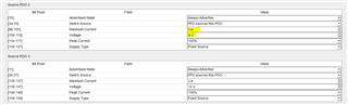
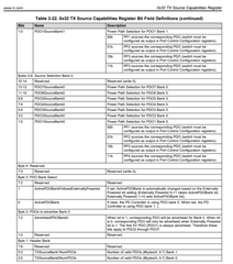
USB_PD:38 [PORT{0-1}]
Id TPS6598X_REG[0] Offset Width Value
-------------------------------------------------------
[24] PORT_CONFIGURATION 0x0028 8 0x0000000033363109
-------------------------------------------------------
< 1> PORT_CONFIGURATION.PORT_CONFIGURATION_TYPECSTATEMACHINE 0:1 0x0000000000000001
< 2> PORT_CONFIGURATION.PORT_CONFIGURATION_RECEPTACLETYPE 3:5 0x0000000000000001
< 3> PORT_CONFIGURATION.PORT_CONFIGURATION_AUDIOACCESSORYSUPPORT 6:6 0x0000000000000000
< 4> PORT_CONFIGURATION.PORT_CONFIGURATION_DEBUGACCESSORYSUPPORT 7:7 0x0000000000000000
< 5> PORT_CONFIGURATION.PORT_CONFIGURATION_SUPPORTTYPECOPTIONS 8:9 0x0000000000000001
< 6> PORT_CONFIGURATION.PORT_CONFIGURATION_VCONNSUPPORTED 11:12 0x0000000000000002
< 7> PORT_CONFIGURATION.PORT_CONFIGURATION_USB3RATE 13:14 0x0000000000000001
< 8> PORT_CONFIGURATION.VBUS_UVP_OVP_SS_VBUS_SETUVPTO4P5V 16:16 0x0000000000000000
< 9> PORT_CONFIGURATION.VBUS_UVP_OVP_SS_VBUS_UVPTRIPPOINT5V 17:19 0x0000000000000003
<10> PORT_CONFIGURATION.VBUS_UVP_OVP_SS_VBUS_UVPTRIPHV 20:22 0x0000000000000003
<11> PORT_CONFIGURATION.VBUS_UVP_OVP_SS_VBUS_OVPTRIPPOINT 23:28 0x0000000000000026
<12> PORT_CONFIGURATION.VBUS_UVP_OVP_SS_VBUS_OVPUSAGE 29:30 0x0000000000000001
<13> PORT_CONFIGURATION.VBUS_UVP_OVP_SS_VBUS_HIGHVOLTAGEWAR_NINGLEVEL 31:31 0x0000000000000000
<14> PORT_CONFIGURATION.VBUS_UVP_OVP_SS_VBUS_LOWVOLTAGEWARN_INGLEVEL 32:32 0x0000000000000000
<15> PORT_CONFIGURATION.VBUS_UVP_OVP_SS_SOFTSTART 33:34 0x0000000000000000
<16> PORT_CONFIGURATION.VBUS_UVP_OVP_SS_ENABLEUVPDEBOUNCE 36:36 0x0000000000000000
<17> PORT_CONFIGURATION.VOLTAGETHRESASSINKCON_TRACT 40:47 0x0000000000000000
<18> PORT_CONFIGURATION.POWERTHRESASSOURCECO_NTRACT 48:55 0x0000000000000000
-----------------------------------------------------------------------------------------------
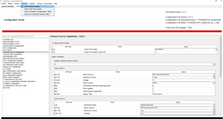
USB_PD:38 [PORT{0-1}]
Id TPS6598X_REG[0] Offset Width Value
--------------------------------------------
[25] PORT_CONTROL 0x0029 4 0x0009c0c2
--------------------------------------------
< 1> PORT_CONTROL.TYPECCURRENT 0:1 0x00000002
< 2> PORT_CONTROL.DISABLEPD 2:3 0x00000000
< 3> PORT_CONTROL.PROCESSSWAPTOSINK 4:4 0x00000000
< 4> PORT_CONTROL.INITIATESWAPTOSINK 5:5 0x00000000
< 5> PORT_CONTROL.PROCESSSWAPTOSOURC_E 6:6 0x00000001
< 6> PORT_CONTROL.INITIATESWAPTOSOURCE 7:7 0x00000001
< 7> PORT_CONTROL.PROCESSVCONNSWAP 10:10 0x00000000
< 8> PORT_CONTROL.PROCESSSWAPTOUFP 12:12 0x00000000
< 9> PORT_CONTROL.INITIATESWAPTOUFP 13:13 0x00000000
<10> PORT_CONTROL.PROCESSSWAPTODFP 14:14 0x00000001
<11> PORT_CONTROL.INITIATESWAPTODFP 15:15 0x00000001
<12> PORT_CONTROL.AUTOMATICIDREQUEST 16:16 0x00000001
<13> PORT_CONTROL.FORCEUSB3GEN1 18:18 0x00000000
<14> PORT_CONTROL.EXTERNALLYPOWERED 19:19 0x00000001
<15> PORT_CONTROL.AUTOMATICSINKCAPREQ_UEST 20:20 0x00000000
<16> PORT_CONTROL.SINKCONTROLBIT 21:21 0x00000000
<17> PORT_CONTROL.RESISTOR15KPRESENT 24:24 0x00000000
<18> PORT_CONTROL.DCDENABLE 25:25 0x00000000
<19> PORT_CONTROL.CHARGERADVERTISEENABL_E 26:28 0x00000000
<20> PORT_CONTROL.USBDISABLE 29:29 0x00000000
<21> PORT_CONTROL.CHARGERDETECTENABLE 30:31 0x00000000
------------------------------------------------------------
Thanks,
Sofian