This thread has been locked.

If you have a related question, please click the "Ask a related question" button in the top right corner. The newly created question will be automatically linked to this question.

TPS546D24A: Question about TPS546D24A Low FET damage

Part Number: TPS546D24A

The answer was late. sorry

- Is this part of a multi-phase stack or a stand-alone single phase application? Stand-alone single phase is applied.

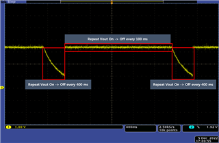
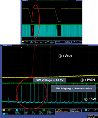
[Question] If Vout is On in [01H] Operation before complete discharge, the ringing phenomenon of SW Pin occurs.
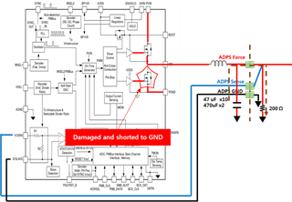
 Could it be a device problem (Low FET Damaged and shorted to GND)?

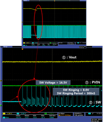
 [Refer to] If Vout is turned on in [01H] Operation after complete discharge, there is no ringing phenomenon of SW Pin. (SOFT_OFF Enable)

Thanks for the help i look forward to your answer

  • Hi Hyun Joo,

    1. TPS546D24A is a stand-alone single phase device and can be up to 4x stackable. 

    2. Operation turn on before Vout complete discharge: That means the pre-biased output start up, TPS546D24A is operating in DCM mode to prevent the low-side FET from sinking current from a pre-biased output voltage. This is expected behavior. The switching ringing is nature of DCM mode of buck converter. 

    3. Operation turn on after Vout complete discharge: That means normal start up with CCM mode. So no SW ringing shows up. It is expected behavior as well.

    Hope this helps,

    Thanks,

    Nancy 

  • Dear Nancy.

    Thanks for your help.

    We are now looking for a very intermittent low side MOSFET breakage.

    If the corresponding DCM function occurs repeatedly,

    that is,

    If repeated control such as OPERATION ON --> OPERATION OFF --> OPERATION ON --> OPERATION OFF is repeated,

    The effect of damage among the characteristics of DCM or CCM is inquired.

    Thanks.

  •  

    Discontinuous Conduction Mode (DCM) operation occurs when the low-side FET is in the OFF-state and the inductor current falls to zero.  The ringing on the SW node occurs when the MOSFET's body-diode shuts off at zero current but there is still a voltage across the inductor.  The voltage drives a current to build up which then oscillates between the parasitic capacitance and inductance of the switching node.  It is not typically a source of MOSFET failure.

    The highest possible stress caused by repeatedly turning the TPS546D24A On and Off would result if the output voltage does not discharge and the TPS546D24A completes it's TON_RISE time without generating a high-side MOSFET turn-on.  When that occurs, the low-side FET is turned on to pull VOUT down to trigger a high-side MOSFET ON-time.  Depending on the inductance, output capacitance and compensation loop, as well as the over-charge of the output capacitor, that can trigger a large negative inductor current, which can place higher than normal stress on the low-side FET when the low-side FET turns off to allow the high-side FET to turn on.

    More likely, however, failure of the low-side FET is resulting from high voltage-stress on the switching node (Drain-Source of the low-side FET) due to the peak ringing on the switching node at the turn-on of the high-side FET when under heavily load.  This ringing is a result of parasitic inductance between the PVIN to PGND bypassing and the switching node, which builds up excess current during the charging of the switching node capacitance.  I would recommend reviewing the SW waveforms with careful attention to the rising edge.

    1) Use the PGND ground of the IC as the Ground, a "tip and barrel" measurement is most accurate

    2) Do not use bandwidth limiting on the probe.  The ringing is generally between 50 and 200 MHz and easily skewed by bandwidth limiting

    3) A horizontal scale of 10-50ns is generally preferred

    If the peak stress on the SW to GND voltage is greater than 19.5V, or shows evidence of "clipping" or truncation, I would recommend reviewing:

    1) Snubber Components (R-C from SW to PGND)

    2) PVIN bypass components and placement (This is why TI recommends a 2.2 - 10nF bypass capacitor from PVIN to PGND)

    3) Value of a resistor in series with the 100nF capacitor between SW and BOOT.  Increasing this resistor should reduce peak voltage stress, though the resistor should not be increased above 4.7Ω. 

  • Thank you for answer. Peter

    We looked for cases where SW was over 19.5v, but we couldn't find such a case. (All of the above measurement methods were used.)

    [Peter answer] The highest possible stress caused by repeatedly turning the TPS546D24A On and Off would result if the output voltage does not discharge and the TPS546D24A completes

    Can the low side FET be damaged if the above is used repeatedly and subjected to stress?(The duration of DCM, or Ringing, varies depending on the case, but in some cases it is maintained up to MAX 1ms.)

    We are going to remove the above case by using soft_off, but I would like to ask how many cases.

    Thanks

  •  

    The low-level ringing on the SW during DCM operation does not apply stress to the low-side FET.  During the ringing, the FET is OFF and there is no current flowing through the MOSFET, so there is no stress on the MOSFET.

    During start-up, the low-side FET is operated for limited periods each switching cycle to prevent the TPS546D24A from sinking current through the low-side FET and discharging the pre-biased output voltage.  When there is sufficient inductor current to maintain positive current flow through the MOSFET's body diode through it's OFF period (no low-level ringing observed) the low-side MOSFET is dissipating more heat and potentially exposed to more stress than the DCM which demonstrates the ringing.  That increased thermal heating would apply greater stress than the DCM which demonstrates the ringing.

    If the TPS546D24A completes soft-start without switching, it may then turn-on the low-side FET for a longer period of time than normal switching to discharge the output.  That could result in a large negative inductor current.  When the low-side FET turns off to allow the high-side FET to turn on, the low-side turn-off can cause SW to ring above PVIN, and then charge PVIN, which could result in excessive Vds stress on the low-side FET causing damage.

    Like starting up into a fully pre-biased output, slewing VOUT down rapidly can induce a large negative VOUT current, which can also over-charge PVIN and cause a high Vds stress on the low-side FET.  Are you performing any VOUT adjustments of your design while it's running?

  •  

    Were these TPS546D24A units purchased directly from TI or through a Distributor?

  • Dear Peter

    Thanks for reply

    Are you performing any VOUT adjustments of your design while it's running? --> Vout is fixed at 3.3v, but ON->OFF uses it repeatedly.

    Were these TPS546D24A units purchased directly from TI or through a Distributor? --> Distributor (Arrow)

    [Question] Please provide a detailed explanation of the operation in the following cases.

    When there is sufficient inductor current to maintain positive current flow through the MOSFET's body diode through it's OFF period (no low-level ringing observed)

    For example, does it mean that the operation of Vout as shown below is repeated?

    Thanks

  •  

    [Question] Please provide a detailed explanation of the operation in the following cases.

    When there is sufficient inductor current to maintain positive current flow through the MOSFET's body diode through it's OFF period (no low-level ringing observed)

    Each time the output of the TPS546D24A is enabled, whether after initial start-up, following an EN/UVLO ON-OFF-ON cycle, or following a restart after fault, the Low-side FET is held off until after the first high-side ON time, and after that, the low-side FET's on-time is limited during it's first 128 switching cycles in order to limit any discharge of the output voltage while the control loop transitions from the OFF to ON states.  This prevents the TPS546D24A from discharging a pre-existing or residual voltage on the output.

    After the low-side FET turns off, if there is still current flowing in the inductor, that current flows through the body diode of the low-side FET, driving the switching node to about 0.5V below ground.  Since this drop is higher than the conduction through the MOSFET channel, the power dissipation in the MOSFET is higher than it is during normal conduction.  Repeatedly starting up the output and forcing the TPS546D24A can increase it's thermal stress, though the internal over-temperature protection circuitry should prevent MOSFET damage from this thermal stress.

    One soft-start cycle every 100ms shouldn't be sufficient to damage the low-side FETs through thermal stress.

    Were these TPS546D24A units purchased directly from TI or through a Distributor? --> Distributor (Arrow)

    Have the damaged devices been returned to Arrow for failure analysis?

    Are you able to share your schematic?

  • Dear Peter

    Thanks for answer 

    but.....

    I don't quite understand the concept of the low-side FET's body diode in any of the phrases below. Can you explain with a picture?

    After the low-side FET turns off, if there is still current flowing in the inductor, that current flows through the body diode of the low-side FET, driving the switching node to about 0.5V below ground

    And there was an error in the picture. Not 100 ms, but ON-OFF in 1 ms or less.

    I will send you the circuit diagram if you send me your mail.

    Defective products will also be delivered through the arrow.

    Thanks

  •  

    I don't quite understand the concept of the low-side FET's body diode in any of the phrases below. Can you explain with a picture?

    After the low-side FET turns off, if there is still current flowing in the inductor, that current flows through the body diode of the low-side FET, driving the switching node to about 0.5V below ground

    Hopefully this will help:

    MOSFETs have Body-Drain Diodes.  When the MOSFET is connected with Source-Body connected, there is a Source-Drain "Body Diode" across the MOSFET.  When there is positive inductor current flowing out of the SW node and the low-side FET turns off, the inductor forces the current to continue flowing out of the SW node, reducing it's voltage.

    When the SW voltage drops to about 0.5V below PGND, the Source-Drain diode is forward biased and the switch node is "clamped" at this diode forward drop below PGND until:

    1) The inductor current falls to 0A, turning off the Source-Drain diode.  At this point the SW voltage is 0V and the inductor current is 0A.  Since the output voltage is not 0V, a small negative current it built up in the inductor to charge the SW capacitance to be equal to VOUT, which starts the resonant ringing you observe on SW during Discontinuous Conduction Mode (DCM) operation.

    2) The high-side MOSFET is turned on, pulling SW up to PVIN

    3) The low-side MOSFET is turned on, reducing the drop from PGND to SW to near 0V

    And there was an error in the picture. Not 100 ms, but ON-OFF in 1 ms or less.

    The Oscilloscope screen shot shows 400ms / division.  At a 1ms On-Off-On repetition rate, the TPS546D24A would not fully turn on.

    With the output voltage discharge rate shown in the oscillscope waveform, if EN/UVLO was "OFF" for 1ms, the output would likely not be discharged at all, which could be inducing the restart state I discribed before where the TPS546D24A completes TON_RISE without generating a high-side ON-time.  That could be triggering a strong discharge of VOUT and the build up of significant negative inductor current before the low-side FET is turned off.  That could induce  high Vds stress on the low-side FET.

    I will send you the circuit diagram if you send me your mail.

    Can you share the schematic through TI's Engineer to Engineer Forum messenger?

    I will send you a friend invite.

  •  

    Are you still looking for assistance on this issue?

  • Dear Peter

     We tried the tip and barrel method, but sw could not measure more than 19.5V. (measured max 16.5V)

    I still don't understand clearly whether device damage is occurring due to the accumulation of instantaneous on of the LFET Body diode during SW Ringing, but thank you for your help.

    I will send you the circuit diagram.
    - Please check.

    And where can I send the defective device through the arrow?

    If you have any additional questions, we will contact you.

    Thanks

  • For TI devices purchased through a distributor, you need to contact the distributor regarding the return material policy.

    Thank you for sharing your schematic through messenger, see my comments there.  The use of the ground symbols concerns me.  If the AGND marked ground symbol that is used for PVIN, PGND, and VOUT ground returns is not the system ground / internal ground layers, there may not be sufficient power-ground copper to support the high currents flowing in the ground, or the MOSFET power dissipation, which could be the reason for the MOSFET damage.

  • Deart Peter

    - We will contact the distributor directly.

    - We have AGND connected to Main GND. The PLANE is designed for more than 50A.

    And we will proceed with mass production by modifying Vout to be used after full discharge.

    And if you still have problems, ask me one more time

     Thank you for your many reviews and advice.