This thread has been locked.

If you have a related question, please click the "Ask a related question" button in the top right corner. The newly created question will be automatically linked to this question.

LM5113: Issue with HI side driver

Part Number: LM5113
Other Parts Discussed in Thread: LM5025, LM5025C

Hi, I´m using a LM5113 to make a DCDC Buck converter like AN-2149 LM5113 Evaluation Board.
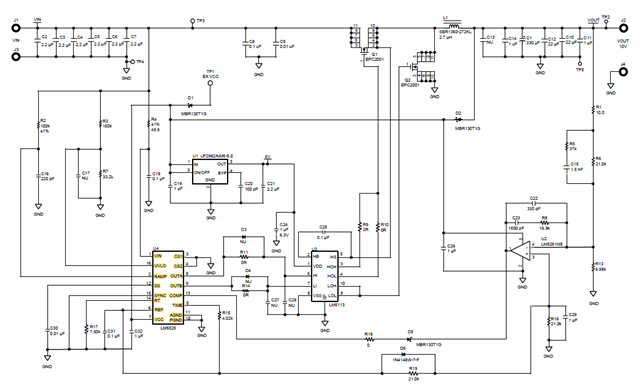
I modificated the circuit to have a 24V output with 48V in the input changing the error stage. It was working without load when with an input of 36V and 24V in the output, C25 broke.

The signal to drive the HI side is like that:

Whe the LI side is:

Any idea why LM5113 broke?

Now I change the LM5113 and C25 and the signal it´s the same. I need to check Q1 but it´s normal this signal if Q1 it is broken?

  • Hi Javier,

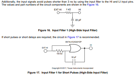
    Thank you for reaching out! It looks like you are experiencing a lot of noise on your high side input pin. I would recommend implementing an RC filter as shown in the LM5113 datasheet:

    It looks like the transient voltage when the HI side tries to turn on reaches a max of 25.5V, and the recommended max on this driver's HI/LI input is 15V. This is likely what damaged the device. An RC filter should help the driver receive clearer waveforms at the inputs.

    Best,

    Alex Weaver

  • Hi Alex,

    This is the signal on the pin 6 (HI) of the LM5113, It is a clean signal without noise.

    I checked Q1 and it switch normally.

    Tomorrow I´m going to put this RC filter in HI pin and I tell you.

    Thanks

  • Hi Javier,

    I misunderstood the labeling of your waveforms. It looks like your HI input signal is clean, so no need for the addition of an RC filter.

    I believe the waveform in your original post is referencing HO (high side output). During reverse recovery, the switch node voltage can drop to negative values. The voltage spikes at the switch node can cause interference to other parts of the circuit. This could be what is causing the strange looking high side waveform. To help with this, consider adding a Schottky diode to help with reverse recovery. Schottky diodes do not experience reverse recovery like the internal body diodes of the drivers, so the alternate current path can help deal with the current flow very rapidly. This should help lead to less of a voltage drop at the switch node, and ultimately less interference to the rest of the circuit.

    Let me know if this helps improve the output!

    Best,

    Alex Weaver

  • Hi Alex,

    I try with the Schottky diode and the result is the same.

    Q1 is not working well, i´m going to change it and tell you about.

    My hypothesis is that the break in C25 raised Vgs above 6 volts and the transistor broke.

    I will be back with good news, I hope

  • Hi Javier,

    I'm sorry to hear the Schottky diode did not help improve the waveform. Please let me know if replacing Q1 improves the results.

    Best,

    Alex Weaver

  • Hi Alex,

    I change Q1 and the result is the same, now if I connect the LM5113 I have a shortcircuit between gate and source.

    EPC tell me the following:

    I´m going to try this and if this don´t work I change for other LM5113

  • Hi Javier,

    Thank you for the update! This will be a good method to help evaluate if the issue is internal to the driver or caused by the external circuitry.

    I will continue to explore potential solutions with the team, and please continue to update me on your debugging progress!

    Best,

    Alex W

  • Hello guys,

    I am actually very interested in seeing if this actually corrected the issue? I have been experiencing the exact same thing for a while now. The zener diode looks like a great idea

     hope to hear back, that this helped you make progress. Thanks

  • I am actually very interested in seeing if this actually corrected the issue? I have been experiencing the exact same thing for a while now. The zener diode looks like a great idea

     hope to hear back, that this helped you make progress. Thanks

  • Hi Arturo,

    I'm not sure if the original author of the post will make an update, but if you start a new post we would be happy to follow up and assist you.

    Best regards,

    Andy Robles

  • Hi Alex,

    I changed the driver and Q1, it works. The broken of C25 damaged both, now is working.

    I have an other problem, to have an output of 24V I change R6 (1,5k) and R13 (12,9k) but I dont have 24V in the output until the input is more than 35V.

    That is normal?

  • Hi Javier,

    I'm glad to hear replacing the driver helped fix the issue!

    Although it looks like you might be able to change R6 and R13 to help modify the output voltage, the AN-2149 LM5113EVM user guide recommends changing R16 to modify the output voltage. Can you try reverting R6 and R13 to their original values and instead changing the R16 resistor to adjust the output voltage?

    Best,

    Alex Weaver

  • Hi Alex,

    If I have an output of 24V, with the original values of R6 and R13, the voltage in R13 will be 5.98V.

    The maximun voltage of Pin 6 of LM5025 (REF) is 5V. 

    Is not possible change R16 for this application or I am wrong?

  • Other question, Is this voltage regulation normal with this driver?

  • Hi Javier,

    On your problem and question: "I have an other problem, to have an output of 24V I change R6 (1,5k) and R13 (12,9k) but I don't have 24V in the output until the input is more than 35V. That is normal?"

    Have you resolved it? If not, I would like to ask if you have ever try to adjust R4 and C18 which are for set up the maximum duty cycle in a design. The EVM is for a 10V output, while yours is for 24V output, so I would think the needed max duty setup is different. If you have not made any adjustment, you may need to do so. You can check the duty with the current setup to see if the duty is always at maximum when Vin < 35V, if so, it would confirm that your problem is due to the maximum duty cycle not set up properly. 

    To know how to set up the max duty, please follow section 7.3.6, 7.3.9 and 8.2.2.3 of LM5025 datasheet. I assume the issue will be resolved so I am clicking TI thinks resolved. If you still need support you can reply so we can continue.

  • I change R4 by 56k but the result it is the same. Changing LM5025 by LM5025C, VIn down to 27V for an exit of 24V but the duty cycle no change if I put more input voltage. The output voltage incress with the input voltage, it is no fixed at 24V. How it is possible? 

  • Hello Javier,

    Alex is out of the office for the moment, he should respond to you by tomorrow.

    Regards,

  • Hi,

    I have replied to your question Vout increase along with Vin on your another thread. Please look into your feedback loop to find if COMP voltage to reduce when your Vout keep increasing. If your LM5025C COMP does not decrease then your feedback loop has something wrong and need to fix.

    "If increase Vin, Vout follows to increase, it looks like your feedback loop does not work properly. When Vout increase LM5025C COMP should be pulled down until the duty cycle changed to make regulation. You need to check your feedback loop work to see where there is something wrong to prevent LM5025C COMP voltage reduction."