This thread has been locked.

If you have a related question, please click the "Ask a related question" button in the top right corner. The newly created question will be automatically linked to this question.

LP5912DRV33EVM: Junction to Pad Thermal Resistance for PowerPad Packages

Part Number: LP5912DRV33EVM
Other Parts Discussed in Thread: LP5912, TPS746-Q1, TPS745-Q1, TPS746

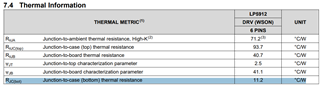
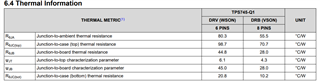
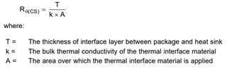
Previously I was able to get information regarding the Junction to Pad thermal resistance for TPS7533QPWP from the HiRel Packaging and Reliability group. We are now looking at a new design considering part LP5912-1.0DRVR, TPS74510PQWDRBRQ1 or TPS74610PQWDRBRQ1 with similar PowePad. I am hoping to also get Junction to Pad thermal resistance for these parts in order to more accurately evaluate the junction temperature in my application. The data sheets only provide junction to case or junction to board information that I do not believe would accurately reflect heat flow through the PowerPad to the board. Use of Theta Junction to Board and Theta Junction to Case results in significant delta temperature between board and case for a device with a PowerPad connection between the two. Our board is also bonded to a heatsink so I believe this would be the primary path of heat flow.

Thank you.

  • Hi Bob, 

    Thank you for reaching out. 

    The Junction-to-Case (bottom) would be the right RJC to use. This is essentially Junction to Pad as the Pad is on the bottom of the case. 

    LP5912:

    TPS745-Q1 and TPS746-Q1:

    The primary path for heatflow will be from the PowerPad to the board: 

    You can reference the following App Note as well: 

    https://www.ti.com/lit/an/snva419c/snva419c.pdf

    Best, 

    Edgar Acosta

  • Edgar,

    Thanks for the info. My concern is that the provided parameters appear to relate back to dissipation to ambient. If Junction-to-Board resistance (40.7 C/W) is used,  the junction temperature higher than the board temperature by 97.7 C based on a 2.4W power dissipation. If junction temperature is 26.9 C higher than case based on Junction-to-case thermal resistance, then the case temperature is 26.9 C below junction (70.8 C)? If so, then despite the thermal pad connecting the case to the board I have 70.8 C difference between the case and the board temp rather than only a few degrees I would expect.

    There is also a distinction in the Junction-to-ambient thermal resistance regarding thermal vias in the datasheet. This makes me think the others (including the Junction-to-case) do not account for this.

    Our board is attached to a heatsink clamped to a coldwall. So the board will be a few degrees above the rail temperature dependent on overall power dissipation. The pad will be connected using thermal vias. During previous application of another part, I was provided data for the Junction-to-pad thermal resistance that was much lower than the Junction-to-case (attached). I was hoping to get that same information for these devices/packages. The heatflow path you provided from the App Report at least shows the via connection to the pad. But it then also shows the heatsink connection to ambient which is not our case. Would these numbers still apply if the heatsink goes to something other than ambient? Is junction-to-case for these really the same as junction-to-pad in the attached (versus junction-to-case in the attached) and its just that much worse in these packages?

    MSP - PowerPAD Thermal Data Table.htm

    Thanks.

    Bob

  • Hi Bob, 

    I have reached out to our thermal modeling team before submitting a request to obtain the Junction to Pad thermal resistance to obtain more clarification on the topic and/or differences between Junction-to-case(bottom) vs Junction-to-Pad. The reason I mentioned the Junction-to-case(bottom) is that the bottom of the case is precisely the exposed pad and the die is attached to this exposed pad. 

    Although for using this parameter one would need to know the temperature of the case at the board since Tj=Tc + (RJC*Pd). Let's ignore the Junction-to-board parameter. 

    Similar to the Junction-to-case(top) :Tj=Tc + (RJC*Pd), Tc is the temperature of the case at the top, therefore, when evaluating using the bottom, this would then need to be Tc at the bottom. 

    For a well-designed thermal layout, RJA is actually the sum of the package junction-to-case (bottom) thermal resistance (RθJCbot) plus the thermal resistance contribution by the PCB copper area acting as a heat sink.

    Now, as already mentioned, PCB will have an impact on any thermal resistance, therefore, we can use the PSI parameters to exclude any PCB dependency. 

    If that is the case, then here are some guidelines for using psi parameters: 

    Can you show how you are doing some of your calculations, and/or how are you obtaining some of the shared values? 

    the case temperature is 26.9 C below junction (70.8 C)

    Also, the numbers shown on the DS are based on a High-K board using JEDEC standards which do include thermal vias. 

    Best, 

    Edgar Acosta

  • The Junction-to-board thermal resistance is 40.7 C/W so at 2.4 W the junction would be 97.7 C above the board. If we assume that the board temperature is 70 C based on our heatsink clamped to a coldwall, then junction would be 167.7C (and thus our concern). If the Junction-to-case thermal resistance is 11.2 C/W, then that would be 26.9 C delta at 2.4W. With heatflow from the junction to the board, I believe that makes the case temperature 97.7 - 26.9 = 70.8 C above board, or 167.7 - 26.9 = 140.8 C in this scenario. So I have case temperature at 140.8 C and board temperature at 70 C when they are tied together by the thermal pad. I'm not sure what that thermal resistance would be but I hope it wouldn't 29 C/W.

    I guess it is possible that the Junction-to-case provided is Junction-to-pad with it just being that much higher due to a smaller package than what we used previously. Is that the correct thing to do in our scenario is ignore Junction-to-board and just do Junction-to-case? This would make case 70 C (maybe a little higher due to board to case resistance). Junction would be 70 + 26.9 = 96.9 C.

    Thanks

    Bob

  • Hi Bob, 

    Thank you for the clarification. 

    After talking with the team and the thermal group, Junction-to-Pad = Junction-to-Case(bottom). This is true for all packages with exposed pads. It is also mentioned in one of the thermal app notes: 

    Semiconductor and IC Package Thermal Metrics (Rev. C) (ti.com)

    Having said that, yes, using Junction-to-Case would provide a closer estimate. Heat will transfer through the lowest resistance path. 

    Furthermore, the heatsink has to also be included to the calculations. 

    The most optimum way to calculate the Tj is as following: 

    This assumes that Rja is known. 

    Also, with good PCB design practices, Rja and Rjc should improve. 

    Best, 

    Edgar Acosta

  • Edgar,

    Thank you for the clarification regarding Junction-to-case and Junction-to-pad for these devices.

    I understand the formula for the board in free air. Would this still apply to our scenario with the heat sink clamped to a temperature controlled coldwall (independent of ambient)? While there would be some heat dissipation to ambient, I do not believe our junction temperature would always be above ambient as our coldwall temperature might be well below the ambient temperature.

    Thanks.

    Bob

  • Hi Bob, 

    To a certain degree. Will this be in an enclosed environment? 

    Agree, some of the heat will be dissipated to the ambient, if this is enclosed there could be some temp rise which could warm the ambient, and if the cold wall only cools one side and does not have any impact on the ambient, then, even if it is small temp rise, it might be worth keeping in mind.

    Although, if the cold wall can help cool the ambient, then this probably wouldn't be applicable and just using the Junction-To-Case would provide an estimate. And/or if the application is in an open environment a similar case following your statement where junction would most likely be below ambient. 

    Best, 

    Edgar Acosta 

  • Edgar,

    And to confirm, we would not use the Junction-to-board thermal resistance in our scenario? 

    Thanks.

    Bob

  • Hi Bob,

    Confirmed. 

    Best, 

    Edgar Acosta

  • Edgar,

    I appreciate your help with all of this. While looking at some different part options, I noticed that there is a TPS746 and a TPS746-Q1. The TPS746-Q1 comes in a larger 8 pin VSON that includes significantly improved thermal performance than the 6 pin WSON for the TPS746. Is the only difference between these two the wettable flank package? I am not familiar with wettable flank. Is there data available on this package? Is it primarily support for inspection with no impact to durability?

    Thanks.

    Bob

  • Hi Bob, 

    The main difference between the TPS746 vs TPS746-Q1 is that the Q1 is AEC-100 qualified material and it comes in two different package options (as you are aware of). 

    Our automotive grade devices go through some extra inspections and qualifications required per AEC-100 Standards. 

    As for the Wettable Flanks, yes, they are primarily to support inspection without impacting durability nor performance. 

    Best, 

    Edgar Acosta