This thread has been locked.

If you have a related question, please click the "Ask a related question" button in the top right corner. The newly created question will be automatically linked to this question.

TPS6594-Q1: TPS65941212RWERQ1

Part Number: TPS6594-Q1

Hello Teams,

Recently, when our product was running at low temperature, TPS65941212 would have a problem of protective shutdown after running at -40℃ for several hours. After this problem occurred, we read the fault register of TPS6594 as shown in the following table:

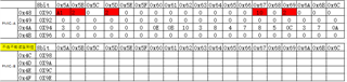
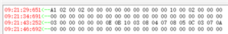
From the test table, we can see that the voltage of BUCK3 is under voltage protection, which leads to the output shutdown of TPS6594 .The detailed register values read are shown in the following table

For this problem, can you provide some relevant technical support?

THANKS and wait fot your reply!

.

  • Hello Derek,

    I see two faults: BUCK3_UV and SPMI_ERR.

    The BUCK3 voltage monitor is tied to the output of the VDD_DDR_1V1 rail in system design. It has a tolerance of +/- 5%. This 1.1V is provided by a discrete resource and not the PMIC. There are 2 options: 1. Improve the circuit design of this discrete resource so that the output voltage doesn't fall below -5% during cold temps. 2. Increase the tolerance on the voltage monitor after boot by writing to the BUCK3_PG_WINDOW register. Because this 1.1V goes to the process, please consult with the Jacinto team to see if this is possible.

    SPMI_ERR is caused by loss of communication between PMIC-A and PMIC-B. Do you lose I2C communication with PMIC-B as well?

    -Mike

  • Hello Michael,

    .PMICA.pdf

    Thanks for your reply  .

    Attached is the latest schematic for this PMICA .You can double check it for us .

    According to your suggestion, we adjusted the threshold range of output voltage(buck1&buck2&buck3) to ±10%, and found that the product that was shut down  as before. We also added a 47UF capacitor to the FB3 power  of VDD2_LPDDR4_1V1, and the two problem products would still run for a period of time and then shut down as before.

    Yes , you are right ,we lost I2C communication with PMIC-B as well .

    When we operated at a high temperature of 85 degrees, the 15 samples all worked normally and no abnormal shutdown phenomenon was found.

    After that , we have found 4 products will shut down after low-temperature operation for a period of time, while the remaining 11 samples can run for 24 hours without shutting down.  

    so ,can you give us some other suggestions for this issue? 

    Thanks .

  • Yes , you are right ,we lost I2C communication with PMIC-B as well .

    Is PMIC-B completely shutting down? This would explain both faults as PMIC-B's GPIO3 controls the DDR 1.1V buck converter in PDN-0B.  

    Based on what you have described, I believe you are seeing a CLK Monitor Fault on PMIC-B on the 4 failing boards. To prove this, after boot at room temp set CLK_MON_SET=0. Then ramp down to negative 40C. 

    The CLK Monitor fault is one of the few errors that immediately puts the digital core and I2C in reset. It is caused by layout and routing sensitivity for the VOUT_LDOVINT capacitor. 

  • Yes,PMIC-B was completely shuting down .

    According to what you said, after we set the register value CLK_MON_SET=0 , we modified the register value (CLK_MON_SET=0) of PMIC-A and PMIC-B at the same time. After that these two problem product , from 11 a.m. low temperature operation to more than 7 p.m. without shutdown, we will add a problem product , let the three product continue to run overnight, if they haven't been shut down, it means that this modification is effective.

    We now have a question, after this register value is set (CLK_MON_SET=0), does it affect other modules or functions? Can we pour this solution into mass production, and are there any other risks in mass production?  

    Attached is the latest PMIC-B's schematic for you double check .

    Thanks .

    PMIC-B.pdf

  • Hello Derek,

    Setting the CLK_MON_SET=0 masks a symptom, the root cause is the sensitivity of VOUT_LDOVINT to layout and placement of its output capacitor. C315, C2992, and C2993 in the PMIC-B schematic. Setting CLK_MON_SET=0 is not meant to be a fix, only a way to identify and confirm the problem. 

    Does the layout, placement and routing of those capacitors follow the guidelines outlined in the data sheet? If not, correcting layout is the best approach to a fixing the problem.

  • Hello Michael,

    Thank you very much for your technical support. After testing and verification, your suggestions and opinions are effective.

    We have three problem products that can run continuously at low temperature for 24 hours without shutting down after changing the register value (CLK_MON_SET=0). It seems that the improvement point is quite effective.
    We would like to ask: if the register is set to 0, what will be the effect? Can we start DV test by this way? Since our DV test plan has been delayed for one month , could you please help evaluate whether we can start the DV experiment by modifying the register value method  CLK_MON_SET=0?
    If we follow the reference design, we don't have to change the register value,  right ? We are worried that the problem of low temperature shutdown will occur again after modifying the routing and placement of the PCB layout.

    Thanks .

  • Hello Derek,

    The clock monitor monitors an internal clock used by the voltage monitor and any glitches could corrupt operation. 

    If we follow the reference design, we don't have to change the register value,  right ? 

    Correct, if the layout follows the instructions in the datasheet, the register value doesn't need change. 

    Can we start DV test by this way? Since our DV test plan has been delayed for one month , could you please help evaluate whether we can start the DV experiment by modifying the register value method  CLK_MON_SET=0?

    Your DV testing may have more failures in other ways if clock monitoring is disabled.

  • Hello Michael,

    We have a question about CLKMON_EN . Can we close CLKMON_EN in mass production ? If it cannot be closed, please explain the reason why it cannot be closed, thank you ! Meanwhile ,Can you explain the main function of CLKMON ?  We want to know the detail `information for this CLKMON register . 

    Michael Gambrill said :Your DV testing may have more failures in other ways if clock monitoring is disabled.

    Can you show me the detail failures information  if clock monitoring is disabled ?  

    Tnanks .

  • Hello Derek,

    The primary concern is the 128kHz and 20MHz internal oscillators and the PMIC sub-systems that use them. With CLKMON_EN=0, voltage monitoring is unreliable and the PMIC may not report a fault when it should. This negatively impacts the ability to achieve ASIL-B or ASIL-D.

  • Dear Michael,

    Thanks for your support!

    i am in the same team with Derek, and working on this issue currently. We've modified layout of PMIC as attached image, could you help to review them for us? Any comments by return will be appreciated!

    Thanks in advance!

     PMIC_A_layout_modify    PMIC_B_layout_modify

  • Hello Tim,

    I will get back to you by the end of the day on Monday.

    -Mike

  • Hello Mike,

    I'm looking forward your response, is there any comments on it?

    Thank you!

  • The ground vias on the caps and the spacing of the VOUT_LDOVINT caps to the PMICs look good.

    -Mike

  • Hi Mike,

    Thank you for your reply!