This thread has been locked.

If you have a related question, please click the "Ask a related question" button in the top right corner. The newly created question will be automatically linked to this question.

BQ24610: Starting a high current battery charger design, is this the right part

Part Number: BQ24610
Other Parts Discussed in Thread: , BQ25730

Hello,

I am new to high current battery charger design but I have a design requirement where the circuit needs to charge a 4P12S battery pack. The design also has a "power path" requirement of being able to deliver 20A to the load source while also charging the battery. I think the BQ24610 could possibly work (though it says that is can support up to 6S batteries). My question is - Is there a better chip for this design and can I use the BQ24610EVM for initial evaluation

  • Hi Mike,

    BQ24610 is only option for standalone (no I2C host required) charging of 4S to 6S battery.  It is a buck charger so it needs an input voltage source higher than the max charge voltage.  The charger's gate drivers were designed and tested for the FET technology available back in 2009. So, we have only tested it (and the EVM is only designed for) up to 10A charging.  Other customers have used it with newer FETs to get higher currents. You might need to add external gate drivers to reach 20A. or you place 2 BQ24610's in parallel.

    We have the BQ25730 family which requires host I2C control and can charge up to 5S batteries.

    Regards,

    Jeff

  • Hi Jefff,

    Thanks for the quick reply... I see that I had a typo but you caught it anyway (The pack is a 4S12P configuration). I am not sure if I can "pump" more than 10A into the batteries during charging so that might be fine but I will look at newer FETs as to reduce the possible heat generation using the older FETs. The 20A requirement is not for charging the battery but driving the load while charging the battery. I was thinking of using a discreet switching circuit that would disconnect the battery path to the load and connect the load to the external power supply, when the circuit detected an external power source. Would like to hear your thoughts on that. And finally when I have completed the design, does TI offer just a quick once over on the circuit to make sure I am in the ballpart.

    Thanks,

    Mike

  • HI Mike,

    The BQ24610 input FETs already connect the system load to the power supply, with the buck charger circuit in parallel to the load.  The battery FET only connects the battery to the load if the input power goes away.  You could a pull down circuit on CE to disable charge if you want all the input power to go to the load. 

    Yes, we can review your schematic once complete.  

    Regards,

    Jeff

  • Hi Jeff,

    Here is a copy of my schematic... I did not compute the values for Iset1, Iset2 and ACSet because I wasn't too sure of the equation, though I listed the operating parameters of the circuit on the schematic. Please let me if there is anything else you need from me to complete your review.

    4087.schematic.pdfThanks,

    Mike

  • Hi Mike,

    The only issue I see on the schematic is D7 being a BAT54.  You might want to change to something capable of more current like the old ZLLS350 on the EVM.  Also, I generally recommend adding a 0ohm resistor between the HIDRV and LODRV pins and the power FET gates.  That zero 0ohm might need to change to 5-10 ohm to reduce ringing at the gate.  

    There is design spreadsheet to help with the resistors at https://www.ti.com/lit/zip/sluc175.

    Regards,

    Jeff

  • Hello Jeff,

    Sorry for the long pause but we finally received our custom boards back and unfortunately their are not working as planned... Perhaps you can help begin to understand the issue. Here are the following steps

    1. We brought the board up in a similar fashion as described in the TI app note sluu396a. We were successful in step 3.41 - AC Adapter detection threshold, where all the listed measurement points read correctly. When we increased the input voltage to 16.V, we noticed that VBAT was only reading 0.741 V. Below are some of the voltage values that might give insight into what might happening.

    ACDRV: ~9.9V

    REGN: 5.99V

    VSYS: 16.4V

    VREF: 3.29V

    Any and all insight would be helpful once again.

    Thanks,

  • Hi Mike,

    Can you send the final schematic with resistors values filled in?  What were the voltages at ACSET, ISET1 and ISET2?

    Regards,

    Jeff

  • Hello Jeff,

    With a VIN set at 18.6V and TS set at 1.8V, I measure the following ISET1 = 0.987V, ISET2 = 0.304V and ACSET = 0.988V. Also attached is our final schematic 

    Regards,

    Mike 

    TheRunner_v5_pg2.pdf

  • Hi Mike,

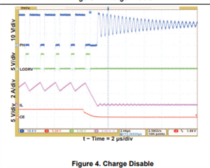
    I don't see anything wrong with the schematic or the DC values.  What is STAT doing?  Is the converter switching, i.e. is there a squarish waveform on the PH node like anything in the plot below:

    I am assuming you don't have a battery attached so I would expect the following:

    Regards,

    Jeff

  • Hi Jeff,

    I do not have a battery attached at the moment but I have CE hard-wired to Vref, so when I look at the circuit the waveforms (PH,LODRV) look more like Figure 2 (Charge enable) from the data sheet.  Could this be the reason why I don't see the representative voltage on VBatt (because I don't have a battery connected at this time). Also STAT1 and STAT2 are both low (battery not detected)

  • Hi Mike,

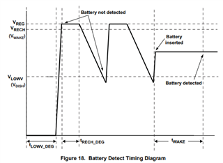
    If battery not attached, you should see a waveform like Figure 18 above, not a low voltage.

    Regards,

    Jeff

  • So that waveform is VBatt, I wasn't sure what it was

  • Hi Mike,

    Yes, if no other issues with the charger and the capacitance in parallel with missing battery isn't too large, then the output should cycle as shown above.

    Regards,

    Jeff

  • Hi Jeff,

    I really appreciate you hanging in there with me while I try to figure this thing out. I took a snapshot of the power up sequence with probes on Vref, VBatt,PH and LODRV. A couple of observations 

    1. The signal amplitude  of PH is 6.2V, while LODRV is 8.8V, VReg is 3.3V and VBatt is 1.34V, not sure what the others should be but VBatt is definitely lower than expected

    2. It seems that the startup waveforms are correct (though the amplitude is not right

    3. The capacitance across the battery terminals is 100uF, which I think is acceptable.

    I hope this gives some insight into what could possibly wrong.

    Thanks,

    Mike

    IMG_1541.pdf

  • Hi Mike,

    Can you check HiDRV?  It should be same as PH except with a dc offset = REGN.

    Regards,

    Jeff

  • Here is a snapshot of PH(Magenta),HIDRV(Cyan) and REGN(Yellow)...As you can see the offset from PH to HIDRV is only 1.4V where REGN is 6V. IMG_1543.pdf

  • Hi Mike,

    I think something is wrong with the BTST capacitor.  Can you remove and replace?

    Regards,

    Jeff

  • I am assuming you are referring to the capacitor between BTST and PH... I changed it and no change in the output but do you think it could be the Diode between BTST and REGN

  • Hi Mike,

    Yes, it could be the diode.  

    Regards,

    Jeff

  • Jeff,

    So that I know what I am looking for... you said under normal conditions, HIDRV should be offset from PH by a DC offset equal to REGN and that the capacitor and possibly the diode could be affecting it. Can you share some more insight into what could possibly be suppressing the voltage levels. I know that a big open ended question but I think I am missing something fundamental to my design.

    Thanks,

    Mike

  • Hi Mike,

    BTST cap, with low side at REGN, has high side of REGN + PH so that it can turn on the high side NFET, in other words, the NFET gate should be REGN volts higher than the input voltage = top of the PH pulse.

    Regards,

    Jeff

  • Jeff,

    Thanks for the explanation, that being said I am honestly at a lost on how to pursue next. Another datapoint is we powered up a second board and initially it demonstrated that same behavior as the first board till we inserted a battery and the board has taken a step backwards. The voltage on REGN is now 10.8V with a Vin of 16.5V (Go figure) Don't know if this helps or am I just confusing the issue.

  • HI Mike,

    REGN is the output of a linear regulator.  If it is out of regulation then either the IC is damaged or you have a short that is connecting a higher voltage to the output of a higher voltage to REGN.  Can you order an BQ24610EVM and modify it with your components then measure all of the voltages and compare?

    Regards,

    Jeff

  • I agree so I placed the order today for the EVM, it will get here in a couple of days so till then, I probably won't bother you. Thanks for all your help so far.

    Regards,

    Mike

  • Ok.  Keep me posted.  Good luck.

    Jeff

  • Hi Jeff,

    I was able to get the circuit operational (finally)..it ended up being the cap coming off BTST and PH, replaced it and now its working (somewhat). Which leads me to my next question. In my application, the AV input is a 18V30A power supply and the battery pack is 3S10P module. I would like to pump 8-10A into the battery during rapid charging and the system load will vary from 5 to 10A. so it seem to me that I need to disable the chip's DPM feature but I still want to keep the PowerPath control, is my assumption correct

  • Hi Mike,

    Glad to hear it.  The IINDPM feature only limits the output current of the converter, i.e. limits the charge current.  So, you could disable the IINDPM by shorting the RAC resistor or you could increase it to 10A + 3*4.2V*10A/18V/efficiency.  The power path feature that turns on the BATFET when input power is removed works the same either way.

    Regards,

    Jeff

  • Hi Jeff,

    So I am putting our custom board through its paces and a couple of observations/questions.

    1. The final battery configuration is a 3P12S and we have updated the resistors accordingly.

    2. When the unit is only charging the battery via the external power supply, the circuit performs as expected. The external supply's current ranges from ~8A down to less than 1 amp during the charge cycle. 

    3. When the unit is in full operation, the unit requires ~15A - 20A, what we have observed is that the battery is supplying all the current necessary and the external supply is not supplying anything. My expectations is that the external supply would provide all the current necessary and use any remaining current to charge the battery. Is that a wrong assumption.

    Regards,

    Mike 

  • Hi Mike,

    The battery should be at least a diode drop below the system = PWR_IN - I(SYS)*Rdson(ACFET).  As long as the VCC voltage is greater than the SRN voltage, BQ2461x enables the ACFET and disables BATFET.  So, is the VCC voltage dropping below the battery voltage and BATFET is turning on? 

    Regards,

    Jeff  

  • Jeff,

    So PWR_IN = 18V, VCC = 17.4V, VBatt = 11.2V, Vsys = 10.9V and  BATTDRV = 5.99V

  • Hi Mike,

    I don't understand how BATTDRV is low, meaning BATFET is on but the VCC>VBATT at SRN.  Any chance you can pull up STATx and PG so we can get more info on the exact fault?

    Regards,

    Jeff