This thread has been locked.

If you have a related question, please click the "Ask a related question" button in the top right corner. The newly created question will be automatically linked to this question.

LM5146: Lowside Mosfets are hot under heavy loads

Expert 1055 points
Part Number: LM5146

Hi team,

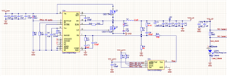
    My schematic diagram of the circuit is as follows. I found that loweside mosfets were heating badly in heavy-duty mode, and measured LO output waveforms separately.


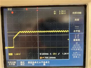
   First of all, when the output voltage is 1.35v and the load current is 0.85A, the temperature of Q3 is 46℃ and the output waveform of LO is measured as follows, it can be seen that the opening time of Q3 is inconsistent, which is unreasonable

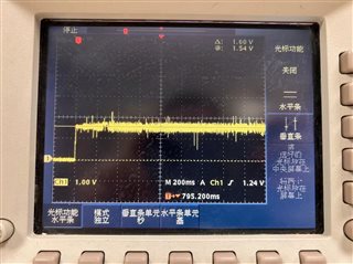
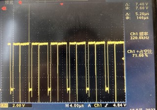
Then I adjusted the output voltage to 1.45V, the load current to 3.8A, and the temperature of Q3 rose to 100℃ within 10 seconds. At this time, the LO output waveform was measured as shown in the figure below, and it was found that the turn-on time side of lowside mosfet was longer.

when I have replaced LM5146, highside and lowside MosFeTs respectively. Serious fever still exists in Q3 under heavy load. Please help me analyze the cause.

  • Hi Suy,

    I'm not sure your comp values are stable with that 1mF capacitance. 

    What is the ESR on that??

    The stability depends on output capacitance, ESR, and compensation values.

    Use the quickstart calculator to help with stability https://www.ti.com/tool/LM5146DESIGN-CALC 

    Also be sure your layout around the low-side FET is able to sink heat. 

    That is the GND polygon needs to connect to a large copper area, and then also heat spreading vias should help.

    Hope this helps,

    -Orlando

  • Hi Murray,

     My PCB board did not paste the 1mf capacitance now.And the compensation values is calculated by the lm5146 quickstart.

    Compared with the PCB of the previous version, the layout was basically unchanged, but the heat of the PCB of my previous version was only about 60 degrees Celsius under heavy load.

  • Hi Suy,

    Please attach the quickstart calculator you used.

    Did you previous layout use these FETs as well?

    -Orlando

  • Hi Orlando,

      Here is the quickstart used,Here is the quickstart used, the same parameters used in the previous design.

    LM5146-Q1 Quickstart Tool r2 - 12Vin 1.65Vout 10A 320kHz.xlsm

  • Hi Suy, your compensation looks good.

    Are there additional capacitances downstream on VCC_LD node? Be sure to use to total effective capacitance and ESR on this node.

    You didnt de-rate the capacitance but I guess it may not derate much at 1.65V

    What about the layout? Are the comp and FB components close to the IC pins? Can you share this placement?

    -Orlando

  • Hi Orlando,

       The total output capacitance is 24uf with no additional capacitance.
       Attached is the layout file.

    1651.top.pdf5807.bot.pdf

  • Hi Orlando,   

       Today's test i found that mosfet heating only in about 10 seconds after power-on and the temperature rose to 110℃, at this time DC power‘s total input power of 14W (load current is 8A), then mosfet temperature began to drop and stabilized at about 75℃, the total input power of DC power is 9W. In other words, mosfet heating is caused by the power consumption of 5w, and the phenomenon still exists by adjusting the time of softstart.

       In addition, when using a fan to cool the mosfet, it is found that the temperature of mosfet is lower than 70℃, and the temperature begins to rise. At same time, the input current of the DC power supply also increases, and then the previous phenomenon is repeated.

  • Hi Suy,

    I looks like you dont have much copper of GND plane connected to low-side FET, the GND plane copper is important as it also functions as a thermal conductor to pull heat from the low-side FET. Did you previous design have more GND copper?

    However your switch waveform does not look stable, the frequency should be stable and duty cycle should be consistent. 

    Did you try this without the VCC LD connected? I'm not sure if thats interfering with the COMP loop.

    Actually your RILIM resistor looks oversized. Based on a 1.19mΩ RDSON of low-side FET, you should have a smaller RILIM resistor of 63Ω.

    This might be the problem with stability.

    Regarding layout:

    • Lower FB resistor RFBB should connect to AGND on the same layer, not sure why you used two separate vias there.
    • I think AGND is best connected to GND at a single point underneath DAP, and then the DAP connected to GND elsewhere.
    • HO and LO traces should be 20mils thick. It's best if their short traces, like FETs close to IC, so that there is minimum gate resistance.
    • Try using a CILIM capacitor to reduce noise on ILIM pin. See quickstart schematic.

    Hope this helps,

    -Orlando

  • Hi Orlando,   

        The copper of GND plane connected to low-side FET in my previous design was similar to the present.Attached is the layout of previous design.

         3872.top.pdf

        When the output is not connected to the load, the lowside mosfet is not hot, but the FB voltage becomes 1.2V. For the RILIM resistance, there is no change in the resistance value by 63ohm.

         Modify. The parameters of the COMP network are different between the previous design and the current design. All components of the previous PCB board are replaced with those used in the current design, and the load (load current 7A) does not appear overheating. So I still don't understand why.
    As for your suggestions on layout, I will carry them out in the next version of design

  • Hi Suy, 

    I'm still not sure the root cause of the issue, however the FB node should not be 1.2V, it should be 0.8V, regulating to VREF.

    Can you show the SW node waveform at no-load, and also at SW node when it's unstable?

    If you are able to use a current loop and a current probe on the output inductor that would be useful information.

    Let me know,

    -Orlando

  • Hi Orlando,  

       I found that the drive signal of lowside mosfet could not be measured when unloaded, but the VCC_LD did have an output voltage although the output voltage was wrong (Vref is 1.2V);
    After the load is connected, the Vref is 0.8V, and the VCC_LD output is the correctly set voltage. When starting, the drive signal of the lowside mosfet heating measuring grid is shown in the figure below


    After more than ten seconds, when mosfet fever is normal, measure the grid drive signal again as shown in the figure below

  • Hi Suy,

    The second waveform looks normal.

    The first waveform is abnormal. 

    I assume you mean VFB was 1.2V? Vref cannot be measured as it is internal. 

    When VFB was 1.2V, was the output voltage over the normal 1.65V? 

    Is there overshoot at startup? Can you measure the VOUT startup waveform?

    -Orlando

  • Hi Orlando,  

       Yes, for the same group of RFB1/RFB2, when Vref is 1.2V without load, the output voltage is 2.48V, and the output voltage is 1.65V with load.

       The start-up waveform of the output voltage Vout is shown in the figure below, where Figure 1 is the waveform with no load, and Figure 2 is the start-up box with load.