Hi,
I have a power rail requirement of below
| Polarity | Voltage | Load Current | |
| + | 2.5 | 400 | mA |
| - | 2.5 | 400 | mA |
| + | 5 | 620 | mA |
| - | 5 | 330 | mA |
In my current design i depend on non-TI solution where i use a 12V to multi rail buck converter, the converter output is filtered through a CLC filter, with combinations of 0.1uF,4.7uF,0.01uF,47uF
the output then taken to a LDO again the LDO output is maintained with a CLC filter
But still my output is noisy like below
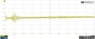
-2.5 Rail
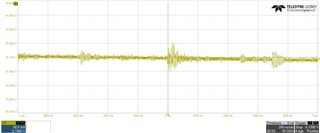
-5V Rail
a wide snap of -2.5v rail
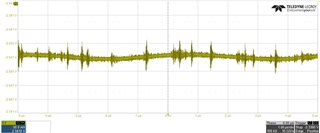
similar nature with the positive rails also
Effective the noise is arround 100mV Peak to peak
i have a amplifier signal chain to which this creates serious problem and i am unable to reduce the reference voltage of A/D conversion due to this problem
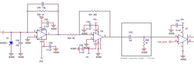
Below is my signal chain
Kindly suggest a power solution for noise sensitive applications like FSO,LIDAR etc.