- Ask a related questionWhat is a related question?A related question is a question created from another question. When the related question is created, it will be automatically linked to the original question.
Hi
I have a query about BQ76930EVM
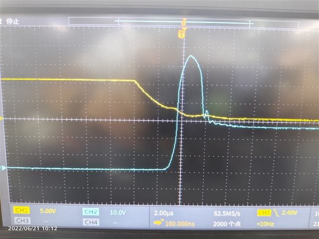
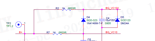
1, The role of R3 and C3 seems to be the same as that of D6. Can I remove D6 or R3 and C3?
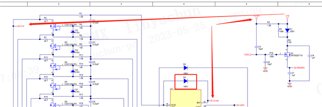
2, What is the function of D42, Q33and Q36?
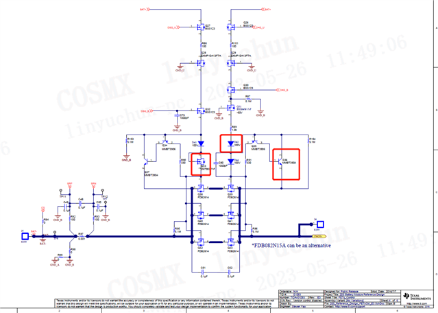
Waiting for your reply.
Thanks
Star