This thread has been locked.

If you have a related question, please click the "Ask a related question" button in the top right corner. The newly created question will be automatically linked to this question.

TPS546D24A: Schematics review

Part Number: TPS546D24A

Hi Team,

I am using TPS546D24A in my design. I would like to get the circuit design get reviewed by experts.
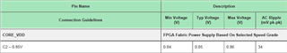
Vin=5V
Vout=0.85V
Iout=120A


I also have few queries regarding the design of the IC.
1. What should be the VSEL resistor value for Vout=0.85V
2. How should the PMBus pins terminated if they are unused in the design.
3. How to terminate MSEL1,MSEL2,VSEL and ADDRSEL pins in stack follower ICs.

Regards,

Shifali N6332.TPS546D24A.pdf

  •  

    I had to edit your post.  You had the wrong part number listed in the title and description.  I have matched the part numbers to your schematic request.

    I am assigning this post to Dani Nadira, who will be able to assist you.

  • Hi Shifali,

    Please fill out the Excel design worksheet and send it back with your design parameters specified, and I would be happy to give a more complete schematic review. I have linked it below.

    In regards to your other queries,

    - For programming VSEL, please refer to section 7.5.2.3 of the part datasheet. Table 7-12 details the resistor divider codes for programming VSEL, and table 7-13 details how to get the resistor to ground code. For Vout = 0.85V, you can program for Vout = [0.5V, 1.25V] with 0.050V resolution, which can be done with a single resistor to ground, or you can program for Vout = [0.75V, 0.9V] with 0.010V resolution, which can be done with a resistor divider. Once you have the resistor codes, table 7-17 will give the corresponding resistor values.

    - For details on stack follower pin configurations for MSEL1, MSEL2, VSEL, ADRSEL, please refer to table 7-5 in the datasheet, which gives the recommended pin connections for standalone, loop controller, and loop follower modes for each of these pins. This table also shows how to configure PMB_CLK and PMB_DATA if they are unused (connect to PGND).

    Best,

    Dani

    Excel Design Worksheet and Schematic Checklist

  • Hi Shifali,

    I will be able to conduct a review on the compensation code and switching frequency elements as well as the power stage once I know your design parameters from the Excel worksheet, but I was able to review the rest of your schematic and here is my initial feedback.

    -Your MSEL2 resistor to ground is not currently configured for a 3-phase stack. See Table 7-11 for more details. For a 3-phase stack with 2 loop followers, use R2G code 2 for your loop controller MSEL2 programming rather than a float. This would result in R1857 as 6.81kΩ.

    -To configure MSEL2 for the two loop followers, use R1878 = 10kΩ and R1879 = 21.5kΩ, which correspond to programming the first and second followers in a 3-phase stack. See Table 7-16 for more details.

    -Since R1848 and R1849 are not populated, and 3.3V_SF_PG comes from off the schematic, I would make sure that 3.3V_SF_PG is being pulled up to a voltage higher than 1.1V to ensure turn on.

    -The AGND pin must be connected directly to the thermal pad on the PCB for each IC. On the schematic, you should connect the AGND pin directly to PGND rather than to R1887.

    -Each IC needs its own separate AGND reference, they should not all be connected to the same AGND. If you require a resistor between the AGNDx net and PGND for net-separation, the resistor should be connected between the AGND pin and the AGNDx net at each device, with the AGND pin connected to PGND so that it can be connected to the exposed pad on the top layer of the PCB with a 0.2mm wide trace.

    Best,
    Dani

  • Hi Dani,

    Thank you so much for your feedbacks.

    Please find the design worksheet with my design parameters updated. Please provide your feedbacks on the same. Also find the attached updated schematics for review.

    Regards,

    Shifali N4812.TPS546D24A.pdfTPS546D24A_TPS546B24A_TPS546A24A_ExcelCalculator_SchematicLayoutChecklist_20200626-designupdate.xlsx

  • Hi Shifali,

    Thank you for providing your design worksheet. I am out of the office today, but I should have my feedback for your schematics ready by Monday.

    Best,

    Dani

  • Hi Shifali,

    I noticed a discrepancy in the switching frequency and compensation code values entered in the design calculator tab vs pin programming tab, which affected the values that were being calculated for further parameters in the worksheet. In your design calculator, your switching frequency was set to 375 kHz and compensation code was set to 10. In your pin programming sheet, your switching frequency was set to 550 kHz and compensation code was set to 1. For the following review I changed switching frequency in the design calculator tab to be 550 kHz to reflect your schematic. Also, VOUT_COMMAND in the pin programming sheet was not entered as your desired VOUT of 0.85V, which was affecting the resistor calculations for VSEL.

    For a switching frequency of 550 kHz, the highest compensation code that can be supported is 9. You can see this in your own worksheet if you change your design targets for Fsw / Fcoi and Fsw / Fcov to less conservative values; I used Fsw / Fcoi = 3.4 and Fsw / Fcov = 7. This compensation code gives a transient response with an output impedance of about 1 mΩ, which will give a drop in output voltage of 1mV per 1A of load current. (for example, for a 30A load current, output voltage would drop by 30mV).

    If your circuit application requires a transient response with less of a drop in output voltage, let us know so we can give additional design recommendations to achieve this, as this would require either more output capacitance, a higher switching frequency, or a combination of both depending on the requirements. If this is the case, please also let us know the part number of the 100uF capacitors being used at the output, as verifying the DC bias derating as well as the ESR of the capacitor is critical for determining the amount of output capacitance needed in the design.

    For a switching frequency of 550 kHz your controller device should have the MSEL1 top resistor as open, and for compensation code 9 the MSEL1 bottom resistor should be 6.81kΩ. See table 7-8 and 7-9 in the datasheet for more details. VSEL should have top resistor open and bottom resistor as 17.8kΩ.

    Best,

    Dani

  • Hi Dani,

    Thank you so much for your feedback.

    1. As per the design sheet, the recommended value for Fsw / Fcov is between 8 to 12. Is there any specific reason for considering 7.
    2. My load IC is an FPGA. Hence it cannot accept voltage drop of 30mV. Voltage drop should be <=5mV. Please suggest design recommendations accordingly.
    3. The 100uF part number is GRM21BR60J107ME15K.
    4. Why did we select compensation code as 9. For switching frequency of 500kHz, I am able to select compensation_code greater than 9 in programming sheet. Should I set it to 9 or select some other value.
    5. ILOOP/VLOOP Ratio in design calculation is 1.28 and is red. Which parameters can be changed in design to avoid this. Is this a major issue?

    Thanks,

    Shifali N

  •  

    is out of the office today, I am assisting her.

    1. As per the design sheet, the recommended value for Fsw / Fcov is between 8 to 12. Is there any specific reason for considering 7.

    Yes, Dani was trying to minimize the output capacitance needed to meet a target transient performance.  The strict requirement is the bandwidth of the VLOOP is less than 1/2 the bandwidth of the ILOOP.  The recommendation of 8 is to keep the VLOOP target less than 1/2 the ILOOP target range of 4.  If VLOOP bandwidth is greater than 1/2 the ILOOP bandwidth, the phase margin of the voltage loop can be low or the loop may be unstable.

    2. My load IC is an FPGA. Hence it cannot accept voltage drop of 30mV. Voltage drop should be <=5mV. Please suggest design recommendations accordingly.

    A 5mV drop on supply voltage is extremely tight during a dynamic load change.  What dynamic load condition requires less than 5mV transient drop?  Are you able to share the power requirement specification for the FPGA?

    3. The 100uF part number is GRM21BR60J107ME15K.

    Thank you.  This Murata capacitor has a +/- 15% tolerance and -9% drop at DC bias of 0.85V.  Accounting for both the minimum effective capacitance is 77μF.

    Additionally, the ESR appears to be 1.6mΩ, updating these two factors in the design calculator will help minimize the number of output capacitors needed to stabilize the loop and met an output transient requirement of 5mV

    4. Why did we select compensation code as 9. For switching frequency of 500kHz, I am able to select compensation_code greater than 9 in programming sheet. Should I set it to 9 or select some other value.

    The Pin Detect Programming tab allows any Pin Programming selection, to know which can work with your application, use the Device Calculator tab.

    Updating the Device Calculator Tab for: 

    Switching Frequency = 550kHz (500kHz is not an option)

    Cer Capacitor Derating = 77%

    Cer Capaccitor ESR = 1.6mΩ 

    Switching Frequency to Iloop Crossover Frequency Ratio (Fcoi) = 3.4

    Switching Frequency to Vloop Crossover Frequency Ratio (Fcov) = 7

    The table in the Device Calculator Tab (J77 - L110) also repeated on Pin Detect Programming Tab P2 through R35) shows the highest VLOOP gain code with neither value red is Code 9 - ILOOP = 3, VLOOP = 4.  This provides the best transient performance available for the provided power-stage (Inductor and Output Capacitors).

    Selecting Code 9 in Device Calculator tab cell E78, shows green for the current loop voltage loop and ILOOP / VLOOP ratio.

    The design tool was left with a 10A load transient and allowable Under/Overshoot of 34mV, so those are green as well, but that does not appear to be accurate.

    The maximum voltage loop gain available through pin-programming is 8x.  With a 3-phase converter, that produces an output impedance of 0.5mΩ, which will meet a 5mV VOUT drop for a 10A load current, but will exceed 5mV for larger dynamic current changes.  If you need to meet an output voltage drop of less than 5mV on a load transient greater than 10A, the deign will require PMBus programming of COMPENSATION_CONFIG and storing of that value to NVM.

    Options for increasing VLOOP to Compensation Code 10:

    1) Increase Output Capacitance

    With the updated derating for the 100μF capacitors, it is possible to meet the requirements of VLOOP = 8 with 10 additional capacitors (52 total)

    2) Increase Switching Frequency

    With the existing Inductor and capacitors, increasing the switching frequency from 550kHz to 750kHz meets the requirements to support Compensation Code 15 (ILOOP = 4, VLOOP = 8)

    3) Increasing Switching Frequency w/ Smaller Inductor

    Increasing the switching frequency to 650kHz and reducing the inductance from 150nH to 120nH, if available, increases the current loop bandwidth using Compensation Code 10 (ILOOP = 3) sufficiently to allow the existing output capacitors to stablize VLOOP = 8.

  • Hi Peter,

    Thank you for the detailed feedback.

    1. I have attached power requirement of FPGA for 0.85V.

    2. Can you suggest an  alternate capacitor part number with better derating value.

    Thanks,

    Shifali N

  • Hi Shifali,

    From your FPGA spec, the AC ripple is 34mV pk-pk, so the device can support a 17mV transient drop.

    Regarding alternate capacitor options, it will be difficult to find a capacitor with a better DC bias derating value in the 0805 package for 100uF. I found a couple of other Murata capacitor options:

    -The GRM31CR60J107KEA8# is a 100uF capacitor in 1206 package, with +/- 10% tolerance and ~4% DC bias derating at 0.85V. This would give a minimum effective capacitance of 86.4uF per capacitor, so you could use about 10% less output capacitors than your previous part with 77uF effective capacitance. 

    -Another option could be the GRM31CR60J227ME11# which is a 220uF capacitor in 1206 package. It has a +/- 20% tolerance and ~8% derating at 0.85V. This would give a minimum effective capacitance of 161.9uF per capacitor, so you could use about 50% less output capacitors. 

    Any of the three ways  detailed will give an output impedance of 0.5mΩ, resulting in a dynamic load current of 35A at 17mV transient drop. 

    1) Increase Output Capacitance

    With the updated derating for the 100μF capacitors, it is possible to meet the requirements of VLOOP = 8 with 10 additional capacitors (52 total)

    For this option (550 kHz and compensation code 10), program MSEL1 with Rtop open, and Rbot = 8.25kΩ. 

    2) Increase Switching Frequency

    With the existing Inductor and capacitors, increasing the switching frequency from 550kHz to 750kHz meets the requirements to support Compensation Code 15 (ILOOP = 4, VLOOP = 8)

    Switching frequency of 750 kHz is not available through pin strapping, the next available switching frequency that could be used to support VLOOP gain = 8 would be 900 kHz. This could actually support compensation code 20, and be done with Rtop = 3.48kΩ and Rbot = 10kΩ. At 900kHz you can also use 10 less output capacitors. If your application could support the extra heat from power loss that would come with increasing switching frequency, this would be an option to decrease solution size. 

    3) Increasing Switching Frequency w/ Smaller Inductor

    Increasing the switching frequency to 650kHz and reducing the inductance from 150nH to 120nH, if available, increases the current loop bandwidth using Compensation Code 10 (ILOOP = 3) sufficiently to allow the existing output capacitors to stablize VLOOP = 8.

    For this option (650 kHz and compensation code 10), program MSEL1 with Rtop = 21.5kΩ, and Rbot = 31.6kΩ. 

    Best,

    Dani

  • Hi Dani,

    I have changed the switching frequency to 650kHz and updated inductor value to 120nH accordingly. I have added additional 6x220uF output capacitors. Please provide your feedbacks on  the same.

    Below are the part numbers considered for Inductor and capacitor.

    Inductor 120nH = PG2110.121HLT

    100uF= GRM21BR60J107ME15K

    220uF= GRM31CR60J227ME11L

    Thanks,

    Shifali NTPS546D24A_TPS546B24A_TPS546A24A_ExcelCalculator_SchematicLayoutChecklist_30062023-designupdate.xlsx2742.TPS546D24A.pdf

  • Hi Shifali,

    Thank you for providing the updated worksheet and schematic. These changes are good for stability and load transient response requirements. With the switching frequency at 650kHz and inductor value at 120nH, the original schematic's output capacitance would even be enough to stabilize VLOOP gain = 8. The additional capacitors don't significantly improve the loop performance, but they are fine to increase stability. The pin strapping is done correctly for all pins and all other schematic elements look good as well.  can give layout recommendations for a layout with this many output capacitors, as layout parasitics can also strongly affect design performance. 

    Best,

    Dani

  • Hi Dani,

    Thank you for the confirmation on schematics. I will share the layout for review once its ready.

    Thanks,

    Shifali N

  • Hi Shifali,

    We would be happy to review your layout once it is ready. If this has resolved your issue for your schematic review, please click "This has resolved my issue" to close this thread, and you can later share your layout for review by starting a new thread. 

    Best,

    Dani