This thread has been locked.

If you have a related question, please click the "Ask a related question" button in the top right corner. The newly created question will be automatically linked to this question.

UCC28070: simulation model for UCC28070 in TINA-TI does not work correctly at 3,4kW

Part Number: UCC28070
Other Parts Discussed in Thread: TINA-TI

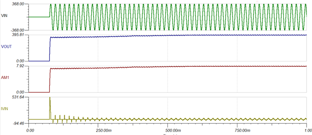
I am currently trying to build a PFC for 3.4 kW.
For this I have built the TINA-TI model and entered the values with the Design Tool.
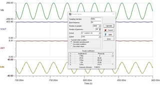
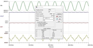
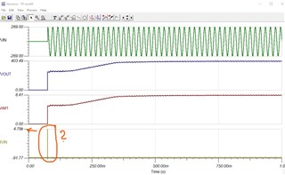
If I start the simulation with an output resistance of 50Ohm to reach 3.4kW, my voltage does not reach the 400V. Also, the current does not look properly sinusoidal at the input.
Can someone help me to find the error?
Attached are pictures and my model.

Here the model.

PFC_3400W.TSCDesign Tool _RevA.xls

  • Hi Philip,

    Please find the attached model which boost upto 400V. The current are effects due to zero crossing distortion which is fine and this comes in TINA simulation because at ZC the current amplifier comes out of saturation which results in these spikes. 

    slum328 (3).tsc

    Regards,

    Harish

  • Hi Harish,

    I checked my model again and found the following.

    In the post e2e.ti.com/.../ucc28070-ti-tina-example-ucc28070_trans
    the user also does not reach the 400V output voltage, as well as a sinusoidal curve.
    The solution there was to halve the resistors R20 and R22 and to adjust the value for CSGAIN with the formula R20/50.
    The reason for this was apparently that the current limit is no longer reached and therefore the 400V can be reached.

    So I have now set the value for R20 and R22 to 5 in my system and CSGAIN = 5/50 = 0.1
    I get the following results for the minimum (Umin=190V --> sqrt(2)*190V = 269V) and maximum input voltage (Umax=260V -->
    sqrt(2)*260V = 368V) at f=50Hz.

    //picture 269V                                                                                            //picture 368V

    But now I still have two questions:

    1. Question:
    When analyzing the Fourier Series, I get for the minimum input voltage (269V) a value for Harmonic distortion of 5.86% but
     for the maximum input voltage a value of 34.4%.
    Why is this value so high? Is this value ok or is there still an error in the system?

    with PF = cos(theta)/sqrt(1+THD) thus results in a value of PF=0.97 for the minimum input voltage and PF=0.86 for the maximum input voltage.


    2. Question:
    Could you explain again why such a high peak input current occurs? Is this ok, or do I have an error here as well?


    Thank you very much,
    Philip

  • Can you please confirm the current sense resistor and CT turns ratio you are using?

  • in the calculation tool I get for a selected value of 50 for the Current sense Transformer Turns ratio a Current sense resistor of 6.8 Ohm.

    in the simulation i use for the Current sense resistor 5 Ohm

    The calculated CT turns ratio is 246. But when i use this value the Harmonic distortion is significantly increased.

  • The spike in current is ok. This is because of the initial conditions of the model. Ideally in a practical circuit there will be a precharge phase where the boost voltage is close to 325V and then the boost stage pumps it to 400V. Also remember there are a lot of approximations in this model for both the converter and boost stage.

    I think you should stick close to the excel/MATHCAD values. If NCT is too low, there may be high power loss in sense resistor and insufficient LM. If too high, there could be excessive LLK and Cd. The THD values are expected to low at high input line voltage and high at low input voltage at full load. I do not expect these values to match board results. These are only tentative numbers which show the trend but please stick with the excel/MATHCAD tool values

  • You sayed:

    "The THD values are expected to low at high input line voltage and high at low input voltage at full load. I do not expect these values to match board results. These are only tentative numbers which show the trend but please stick with the excel/MATHCAD tool values"

    did you make a mistake and mean: THD low at low input voltage and high at high input voltage?
    Because as you can see in my pictures above, the THD value is low at low input voltage with 5% and high at high input voltage with 34%.

    Yes, i work more with the excel sheet, but for a good comparison i want good simulation results.

  • Sorry my mistake.. Yes your rephrased answer is correct

  • ok so my model seems to be correct. However, I am new to this field and wanted to ask again why THD is low at low input voltage and high at high input voltage. Are there any sources to read about this?

  • Hi Philip,

    Your model is correct. The THD numbers are similar to those explained in the following document:

    https://www.onsemi.com/pub/Collateral/HBD853-D.PDF

    https://www.infineon.com/dgdl/an-1173.pdf?fileId=5546d462533600a40153559ad4eb1143

    1. The boost inductor stores enough energy during the inductor charging phase normally. During the inductor discharging (off time) phase, the total capacitance, charges up to the required voltage, which is the output voltage Vout plus the turn-on voltage of the output diode. Once the diode is turned on, the energy stored in the inductor is delivered to the output.

    2. When the line voltage VAC is near the zero-crossings, the inductor can still store the energy during the inductor charging phase, but the energy is too low to charge the switch node up to the required voltage during the inductor discharging phase. As a result, the diode will not be turned on and the energy will be confined in the tank circuit consisting of Csw and Lboost and will be discontinuous for an interval until the absolute value of the line voltage lager than the voltage residual voltage on the bulk capacitor after diode rectifier.

    3. Thus, the diode of the bridge rectifier can’t be turned on and the flat portion in the line input current IAC happens. This distortion is called “crossover distortion”, which increases the number of the total harmonics in the IAC greatly. In other words, the THD becomes serious.

    4. At high line voltage on time is reduced drastically and the amount of energy stored in boost inductance is less and this effect becomes more when compared to low input line voltage.

    5. The crossover distortion may also be deteriorated if the input line rms voltage increases because the output power is fixed and thus the line current becomes lower. It results in large flat portion as depicted in Fig below. The Ilimit is the required current which can charge the switch node up to the required voltage.

    Regards,

    Harish