This thread has been locked.

If you have a related question, please click the "Ask a related question" button in the top right corner. The newly created question will be automatically linked to this question.

LM74900-Q1: LM5074900-Q1: Schematic Review

Part Number: LM74900-Q1
Other Parts Discussed in Thread: LM74900

Hi Team,

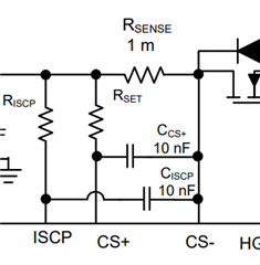
Could you help review the LM74900-Q1 input path schmatic LM74900-Q1.pdf 

The is Infotainment for automotive for using Or-ing, Reverse current blocking, Reverse polarity protection, Overcurrent Protection

Vin 1 & 2 = 12V DC

Load Current = 4.5A at 12V DC

Revers polarity protection test voltage= -14V 

Load Dump  Vmax 32V, tr:300ms,Interval:60s with the 10 Cycle 

  • Hi Sekhar,

    Please see my schematic review comments below,

    1. Change the input TVS from TPSMC27CA to TPSMC36A. The breakdown voltage of the TVS has to be > 35V which is the suppressed load dump voltage. 

    2. VS pin provides power supply to the internal circuits of the IC. Add a 0.1uF capacitor from VS to GND as it helps in EMI performance as well.

    3. For passive component values selection/verification, please use the attached design calculator.

    2577.LM749X0_ID_Design_Calculator.XLSX

    4. In case filtering is required for SCP and OCP, add capacitors across ISCP to CS- and CS+ to CS- as shown below.