This thread has been locked.
If you have a related question, please click the "Ask a related question" button in the top right corner. The newly created question will be automatically linked to this question.
Hello,
I was hoping someone can help me understand the issue here.
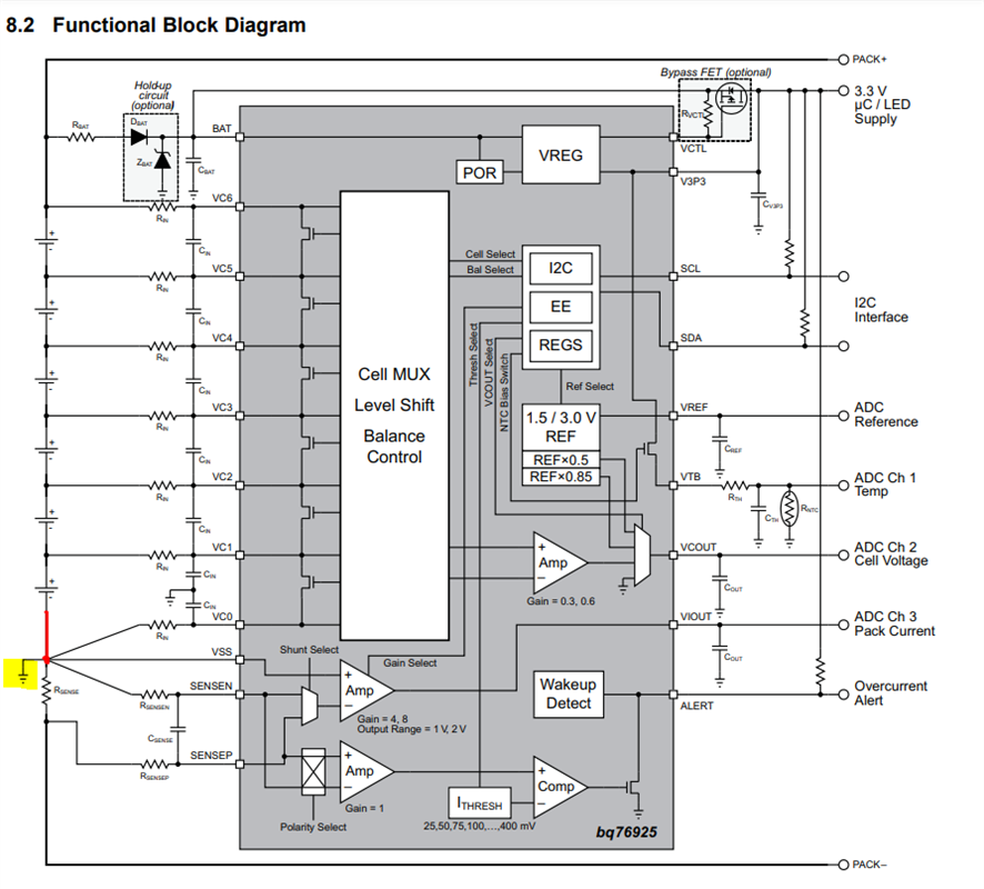
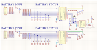
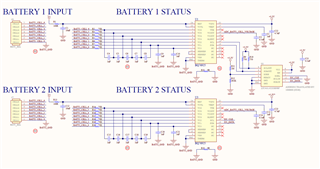
We use 2x BQ76925 in our product to monitor 2x 6S LiPo batteries, strictly as an AFE with no cell balancing, current monitoring or temperature.
We have used this part in production with our previous generation heavily and have never had issues with it.
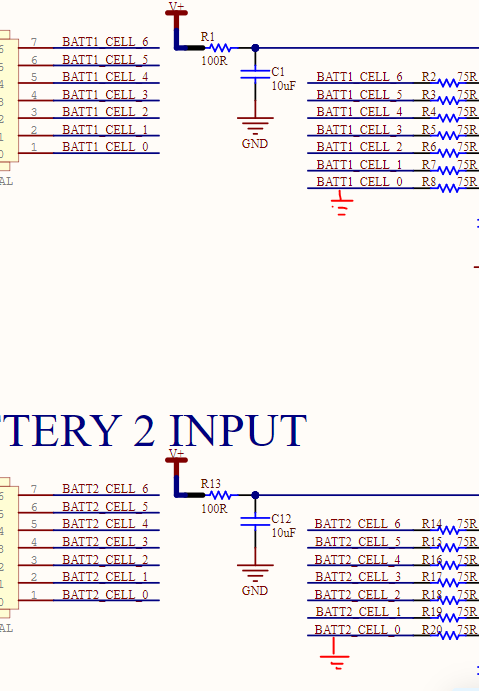
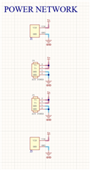
In this generation, I changed the schematic such that Cell 0 is no longer directly connected to system ground when connected (it is floating until main battery leads are connected).
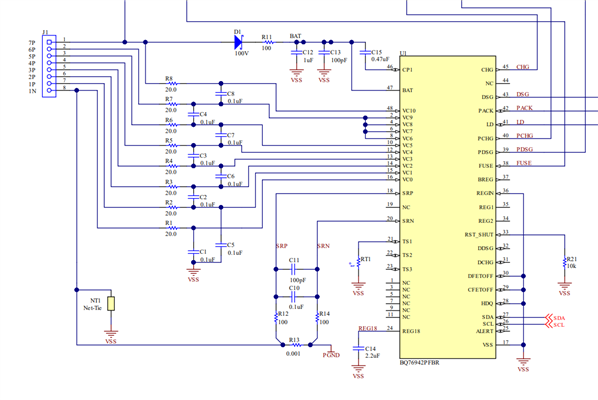
Please see attached Altium schematic file for what it currently is (it mostly follows the EVM, the cell filtering is done with respect to common ground and not in a differential configuration).
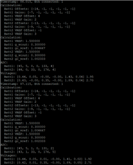
The issue we see here is that Cell 0 of the battery monitor (very random to which chip it occurs on) shows a much lower voltage than anticipated. This issue is very sporadic, but it seems like it degrades further as we connect and disconnect leads and keep using it in our system. We normally connect the balance leads from our LiPo battery first since it is the hardest to reach and then our main power connector.
This is a strange issue because when I do benchtop tests with brand new parts and with 200+ power cycles and connections, I don't see the issue, but once it is assembled into the product, the issue shows up in <50 boot up cycles, maybe quicker. I've tried to muck around with the mechanicals but I don't see a consistency. The issue comes up when it wants to. Once the issue comes up on the chip, it can be replicable after some time on the bench top.
Do you have any idea of where the problem lies?
Hope to hear back soon!
Kind Regards,
Neehar Shah
Hi Neehar,
It is unclear why this may be happening, some data would help to understand the issue you are seeing with VC0.
From the schematic we see that there is no reference to BAT- on the VC0, unless I am missing it. Do you know why that is?
Could you also measure what the differential voltage is between VC1 and VC0 when you see this issue happen?
Any other kind of measurements you can show will help understand the root cause.
Thanks,
-Luis Torres
Hi Luis,
Thanks for your reply and feedback. I apologize for the lack of info, let me try to give some more additional info about this.
To answer your first question, GND is BAT-. There is no separation between BAT- and system level GND as they are common to our system.
I'll give out an example of what I have seen.
So we currently use an arduino based MCU in which it spits out cell voltage readings on a serial port. Our batteries are 6S HV so we can see upto 4.35V per cell in readings. On a working system with a fully charged battery, we see accurate numbers of 4.35V for each cell. In the event this issue occurs with VC0, we see a very low voltage and it varies on random boot cycles. Sometimes we see it is reporting <1V, sometimes it shows around 2V, etc.
I have taken some measurements this morning:
So looks like this morning VC6 is reporting incorrect voltage. I have seen it on either VC0 or VC6 where it reports incorrectly.
I have measured the differential voltage between VC6 and VC5 when it is in a bad state and it reads correctly on the multimeter at 4.11V. In the bad state, the numbers we see is around ~0.45V.
The measurement voltage at the battery pack is 4.13V differential of VC6 and VC5.
I was curious and took a resistance measurement between each VCn pin to the cell pack connector and looks like all are correct to the schematic except for VC1 and VC0. It seems like those two resistors start to degrade significantly. The current measurement that I have from VC1 to the connector is 159Ohms and VC0 to the connector is 347Ohms. A good and untouched board shows 75Ohms nominal. Another board that I had been doing many tests on shows degradation at VC1 with 79Ohms and VC0 at 89Ohms.
Hopefully this additional info is helpful!
Kind Regards,
Neehar
Hi Neehar,
Thanks for the helpful feedback!
While the datasheet does not explicitly state the that VC0 must tied to ground, many of the device diagrams and examples will have the same implementation. The reason being that if the VC0 is left floating it has a chance to see a spike in voltage during assembly which is enough to cause the issues you are seeing with erroneous cell voltages and degradation of the filter network.
Our recommendation is that a proper connection be made between VC0 and GND.
Please let us know if this resolves the issue you are seeing.
Best,
-Luis Torres
Hi Luis,
Thank you for your feedback on this.
So if I was to tie VC0 to GND, that will likely fix the issues? Of course after replacing the chip would this only work.
How about in the case if I was to insert main battery power connector first to have a proper ground and then balance leads? Since VC0 on the battery pack and BATT- are connected internally to the battery, the reference would no longer be floating?
The reason I ask this is because we removed the GND connection from Cell 0 from the circuit as we were having issues with main battery pack connector pin shorting with screws and would like to keep it this way.
I was looking at the evaluation kit schematic, and correct me if I'm wrong but it looks like the schematic I have implemented is the same, the only difference here is the cell filtering is differential and there is current sensing on the eval kit?
So much like the eval schematic, the GND is not directly or indirectly tied to VC0.
I've highlighted the connection in red.
Hi Neehar,
The connection is correct (to a point) but maybe I was a little unclear. Please see the figure below, in your schematic BATT- is not referenced to VC0 at all. While your path does connect it to VSS there needs to be a GND reference to the bottom cell (as in the figure).
In the current schematic I do not see a GND connection, this means that the node can float and may see a voltage exceeding abs max of the pin which can happen at assembly.
This should also address your concern about unexpected shorts so long as you tie it to the board GND.
This should be sufficient, please let me know if you have any other questions/concerns.
Best,
-Luis Torres
Hi Luis,
Thanks for the feedback.
I understand, I see that I am missing the low resistance path through Rsense that provides a GND connection.
Does this also mean that if my order of operation changes from battery pack mains connect and then balance lead connect, that it would solve my issue since balance leads would not longer be floating or does the GND connection still need to be present?
Do you think if I put a low enough resistance (like <10Ohms) that it would be sufficient enough instead of a hard GND connection?
Kind Regards.
Neehar
Hi Neehar,
We recommend the use of a 0ohm resistor to separate the high current path, we do this in our other EVM's to separate the high current path from IC. You can see it implemented here on this BQ76942 typical application schematic as a net-tie to ground.
I'd also like to note that we want the high current path to go through the sense resistor if you are doing any kind of current protections, but I recall you are not using the feature so not an issue in this case.
Best,
-Luis Torres
Hi Luis,
Thank you for your patience while we test this fix. We had a chance to take some new boards we had just received and tie Cell0 to system GND and looks like that has fixed the issue with cell0. But now we have an issue on all of the boards that Cell 5 (between VC4 and VC5) shows an incorrect reading. We are about 700mV lower than what is expected. Only a fully charged cell we normally see ~4.2V, but now I see 3.6V on cell 5 of the battery.
The AFE was working for about a day or so and then started showing errors on Cell 5 readings.
Any idea on where to look for this? The raw ADC values are showing much lower than the other cells when in actuality the cells are balanced and equal at ~4.2V. Measured the voltages before and after the RC network and all voltages are correct. Something weird is happening within the IC that is giving out wrong values.
Kind Regards,
Neehar
HI Neehar,
Its good to hear that the initial issue was resolved. I've rotated out of the applications team and will leave you in good hands with my colleague Luis Hernandez Salomon . Luis can you please help Neehar with the above issue?
Best,
-Luis Torres
Hello Neehar,
Is it inaccurate at all voltages? Or it becomes more inaccurate as it reaches the full cell voltage?
If the IC is replaced, is the issue gone? I am wondering if somehow the IC may have gotten damage, specially since you mention it was working initially.
Best Regards,
Luis Hernandez Salomon
Hi Luis,
It is inaccurate at all cell voltages, whether they are near max or somewhere in the middle the reading is incorrect.
So to give a little additional background, we have two of these ICs on the same board that are our AFE for two batteries and monitor each battery individually. Both ICs are exhibiting the same issues on the same board and on multiple boards. I believe I have attached the original Altium schematic for the two BQ76925 chips.
These were also brand new boards and is being observed on multiple boards which makes me believe it is systemic in nature. It is possible that if I was to replace them they may start working again, but I don't know for how long it will last for.
Kind Regards,
Neehar Shah
Hello Neehar,
That is interesting, so just to confirm the parts are all operating correctly initially, but after some time they start to show inaccuracy in cell 5, correct?
I did see the schematic and it seemed okay to me. Do both of the parts on the board display issues on cell 5? Or just the top or bottom device display the problem? Are you measuring directly at the VC5 - VC4 pins to see if the voltage matches?
Best Regards,
Luis Hernandez Salomon
Hi Luis,
All the parts initially worked for some time (probably a day so I would say about 10 battery connects and disconnects) but now cell 5 (VC5-VC4) cell readings have been incorrect.
Both parts on the board display issues in cell 5 and it also occurs on 3 other boards in our motherboards as well.
I have measured before and after the RC filter with a multimeter and it shows correctly of ~4.2V, however after it is processed through the battery monitor, it no longer provides the correct analog value.
Kind Regards,
Neehar Shah
Hello Neehar,
Were there any register changes before and after? What about the calibration gain/offset values for cell 5? Is there any difference before and after?
Best Regards,
Luis Hernandez Salomon
Hi Luis,
So it is difficult to get results of before the failure of cell reading as we never print out the calibration settings, but it looks like nothing has changed in that respect that is drastic enough to justify the failures we see here. Please see below screenshot for those values and errors we are seeing.
Something interesting showed up during my testing today.
We have used this part heavily in our previous version of the product, in this case the AFE and the MCU exist on the same board. The firmware code for the AFE is exactly the same between the current version and the previous version of the PCB.
What was interesting is that when the balance connector and the power connector are connected to the board, the voltages read perfectly fine. When I remove only the balance leads, the voltages almost immediately go to 0V on each cell (as expected).
When I did the same test on the current version where we are experiencing problems, the voltages slowly decrease cell by cell and some even show increases in voltages which is very weird. So I tried to connect just the main power to the board and it looks like the AFE is showing some voltage without a balance lead connected to it. Please see screenshot of the values below:
Hopefully this can help in what is happening. You'll notice Cell 0 and Cell 5 are showing voltages when they shouldn't be. Also to further note that the firmware has not changed from the working version to this one.
Kind Regards,
Neehar Shah
Hello Neehar,
That is very strange, it is possible the part is getting damaged.
What differences are there between the previous design and this PCB? Are the schematic the same or they different?
Something that may be worth noting, is that I see you are using a single-cap filter capacitors for the input cells, which could potentially cause damage during cell connections. There is an E2E on the topic:
By any chance do you have an EVM that you can test the IC's showing the problem? Just to confirm if there's damage on the IC?
Best Regards,
Luis Hernandez Salomon
Hi Luis,
With the findings that I provided, that actually happens on any of the current versions. So this means that out of box when the AFE is working it will behave the same way as shown above (no balance leads connected will show increasing voltages in certain cells). It is possible that damage is occurring to the AFE but it is happening to every single one we have produced so it seems very systemic and reproducable.
The major difference between both revisions are the following:
- Same schematic (after grounding VC0 to the system)
- Package sizes changed from 0603 to 0402
- Layout and placement is different (following normal DFM strategies as best as possible but this AFE doesn't have major routing restrictions as far as I understand)
- AFE's are separated from MCU and are interacted through board to board mezzanine connector
We have always had single-ended RC circuits on these AFEs and hasn't caused us any trouble. I've been wanting to move to the differential layout but because the former works well we decided to keep it unchanged.
I do have the EVM, what is the best way to connect the chip? We currently use the QFN variant whereas the one on the EVM is SOP.
Is it best to air wire the pins as best as possible to the EVM?
Kind Regards,
Neehar
Helo Neehar,
Package sizes should be okay as long as the parts are rated for the voltages seen. The only condition we have is to separate the high-current path of the battery from the IC and to have filter components as close to the IC as possible. Layout-wise, where is the battery ground flowing?
Are there any ESD components on potential locations were it can be a risk?
I understand, as per the E2E I shared about differential vs. single-ended RC's, there is some risk of damage, although in this case I do find it unlikely that this is the cause of the problem.
That is tricky, but unfortunately for the QFN package it would be the only thing you can do with our EVM, you would have to air-wire it or something of the sort, to use with or EVM.
Best Regards,
Luis Hernandez Salomon
Hi Luis<,
Yes ratings have been selected accordingly for the new package sizing. As for where Battery ground is flowing, currently battery ground and the mother board ground is the same. So the ground for the IC is the same as battery ground. This is also the case for the previous version as well that works perfectly fine. The previous version has been in service for about a year with 0 issues with the AFE and about 30-40 motherboards made.
We have very little ESD components on the board, especially for the AFE we don't have any ESD protection. A lot of the chips and interfaces we use have built in ESD protection when required. It is a fully enclosed system inside of a carbon fiber airframe so electronics are not accessible, only connection to the battery and balance leads.
I agree, I don't think that is the likely cause of this issue, but I do understand the benefits of differential RC in this case.
I can try to air wire the qfn package to the evm and let you know the results. I will hopefully get back to you about this asap!
Are there any specifics you would like to know regarding the EVM when connected? Any screenshots that is useful from the software side of things?
Are there any documents I can share with you that will better help understand? I can share the PCB doc as well if that will help!
Kind Regards,
Neehar
Hello Neehar,
You can share your PCB doc! If you do not want to share it in the forum, you are more than welcome to send me a PM with the file .
You can read the bq76925EVM Evaluation Module User Guide to get an idea as to how the EVM is connected and how to interface to it. I hope we can shed light on what is going on soon!
Best Regards,
Luis Hernandez Salomon
Hi Luis,
I have provided the PCB Layout in a PM to you
I will hopefully have some time to work on this tomorrow morning, I'll keep you updated on what the results are.
Kind Regards,
Neehar
Hello Neehar,
I looked at the layout.
Unless I missed something, I do not see a clear separation between the high-current battery path and the IC ground. So the high current of the battery could flow anywhere on the PCB.
Typically we add a net-tie or 0-Ohm resistor between BAT- and Vss/GND in order to separate the grounds. I would recommend to separate the grounds completely.
Also, are the devices stacked, or in parallel?
Best Regards,
Luis Hernandez Salomon
Hi Luis,
Thanks for checking out the layout.
As for the separation, I believe I mentioned in my previous post that the Battery Ground and IC ground are the same. But something to note of that is that the previous revision of this that does work and is in production has not failed. The previous version also has battery ground and IC ground connected together, there is no separation there.
The board is stacked onto another board. I will send the related files in PM.
Kind Regards,
Neehar
Neehar,
I do understand, but this is just a common recommendation we make as we've seen failures in the past due to not having these separated. This separation is something that it is commonly seen across almost all battery management systems. Maybe this is not causing the current issue, but it is something else to keep in mind!
What differences in layout is there between the previous production and the current one?
I will see the files you sent and send more comments tomorrow! .
Do let me know if you are able to test on the EVM!
Best Regards,
Luis Hernandez Salomon
Hi Luis,
Oh definitely will keep this in mind! We are in the midst of a redesign so I will be taking all of your suggestions and implementing them =)
I believe the major difference in routing is part of the RC filter - R and C are further apart from each other on the current one than in previous.
I appreciate you taking the time to review these things for me, it's quite helpful! As for the EVM, I did the best I could to air wire these pins to the EVM and below are some screenshots from the evaluation software.
The above 2 are with cell sim switches enabled.
The above two are for LiPo batteries that we use.
I am not sure why VC0 is not reporting anything, it is possible I have shorted something in the process and have not noticed, but the values do not correspond to the measured multimeter values of the cells. Cells 3,4,6 are the correct values +/- 1% and is what is measured on all the cells.
I sent this in case there is something telling from this, in the meantime I want to try to do this experiment again with another "damaged" IC but it will likely be late tomorrow or Friday for when I have results.
Looking forward to your reply!
Kind Regards,
Neehar
Hello Neehar,
Yes, it seems cell 1 may have not been properly connected, this probably is why cell 2 is not measuring currently.
I agree, it is more telling that there could've been some damage. Do let us know what the results are!
Best Regards,
Luis Hernandez Salomon
Hi Luis,
So I got my breakout board and did the same tests but with the second AFE that was on the same board.
I believe both of the chips are damaged (as are the other boards that show the same issue).
Please see below for the results:
No balance leads or cell sim connected
Only cell sim connected
LiPo battery connected for voltage readings
As you can see that all instances of connections are showing incorrect values. It is to note that two of the inputs are not reading correctly, mainly VC5 but also VC0. It is also to note that even without any cells connected, upon boot up shows false readings which is never the case as it usually shows near 0 values instantaneously.
I'm not quite sure what the next steps are here.
Kind Regards,
Neehar
Hello Neehar,
Just to let you know, E2E will be down today and the weekend.
So I will give you a response on this on Monday. Apologies for the delay!
Best Regards,
Luis Hernandez Salomon
Hi Luis,
Thank you for letting me know, looking forward to your response today.
Kind Regards,
Neehar
Hello Neehar,
Apologies for the delay, I was out of the office most day yesterday.
On the first case, what exactly is the "balance leads" and "cell sims" shown on the first case? How can these affect the readings so much?
Although the second two images are not completely correct, they seem much better, so I assume that in the first case the voltage on the pins are also similar to what the software is reporting. Is that the case?
Is it possible to create a prototype with revised layout to see if these help? You could also try adding Zeners during assembly at the inputs of the pins to see if helps with making sure these do not fail? I am curious also, in what conditions did you see the parts fail?
Best Regards,
Luis Hernandez Salomon
Hi Luis,
Hope you had a good weekend.
In the first case, this is the chip basically with floating inputs. Nothing is connected to the inputs (i.e. no battery cell connector nor the cell sim switches). I don't have a clue as to why it even has a reading because normally if nothing is connected it is near 0 for each cell.
The second images are definitely much closer and are more realistic. The voltages on the pins themselves are pretty much what VC2, VC3 and VC4 are reporting. The other ones are quite a bit off (>100mV). But weirdly enough, in our firmware it reports VC5 to be nearly 500mV less than expected. The software on our end is slightly off but the trend of which cells are reporting issues is the same. In both cases, our product is not allowed to function.
The AFE is used for battery voltage monitoring on our drone application. From my presumptions, these AFEs fail quicker once operating in the drone. We use the same batteries in our old revision as we do with our new and both provide different results.
A prototype that we did was tying the BATT_GND to system GND which fixed our initial VC0 issue, we would have to create a new design batch that incorporates the 0Ohm resistor between system GND and BATT_GND. It will take around 2 weeks or so to get there. I'll see what else we can do to prototype this as well.
Kind Regards,
Neehar
Hello Neehar,
Hope you had a good weekend too!
Thank you for clarifying. That makes sense.
I hope that this new prototype shows an improvement. My assumption is that the device is getting damaged, maybe due to ESD or transient. It is hard to really know why. I will leave the thread open so you can let me know if there are any other updates!
Best Regards,
Luis Hernandez Salomon
Hi Luis,
We are looking into making this changed as suggested to see if this will alleviate the problem.
I'm going to be working on the schematic either today or tomorrow base don your feedback.
I would like your help and clarification on where the ground separation should occur. We have about 300A of burst current through the system every 10 seconds. The product is powered through the power leads on J1 and J3.
Just referencing battery 1 monitor (which will be copied for battery 2 monitor) for the changes that need to occur:
- C1, C4, C5, C^, C7, C8, C9, C10 will have a new ground (GND_SEP)
- VSS and THERM pins will now be connected to GND_SEP
- BATT1_CELL_0 will now be connected to GND_SEP
- 0 Ohm resistor needs to be added to connect GND_SEP with GND
Do I need to put the grounds from J1 and J3 to GND_SEP as well? I am worried that all the current going through the jumper resistor may pop at some point.
Could you please let me know if this is correct way of doing it?
Kind Regards,
Neehar Shah
Hello Neehar,
That sounds okay to me!
If J1/J3 are where a load/charger would be connected, this would be referring the high-current path, so it would be referenced to GND. Is that the case?
Best Regards,
Luis Hernandez Salomon
Hi Luis,
Yes that is correct, J1/J3 are where our LiPo batteries are connected for main source of power to the system. This is where all high current is sourced from. So then to clarify in this case, J1/J3 should still remain as system GND, but the above changes are OK? If this is correct, then I can start making the changes.
Kind Regards,
Neehar
Hello Neehar,
J1/J3 should still be referencing to the same GND, just separated from the low-current ground (which I assume is GND_SEP) through a 0-Ohm resistor.
Once you make all necessary changes, you can send me a PM and reply here so I am aware!
Best Regards,
Luis Hernandez Salomon
Hi Luis,
I have sent you in PM the updated design, I will be working on the PCB layout right now as well and sending it off for manufacturing.
If you can do a once over to make sure everything is good. I have moved to a differential mode of filtering as well.
I picked an 0402 jumper resistor for this.
Kind Regards,
Neehar
Hello Neehar,
All of the low-current paths should be connected to the low-current ground, so the outputs/communication lines should connect to the low-current ground.
Is the MCU off-board?
Best Regards,
Luis Hernandez Salomon
Hi Luis,
Yes the MCU is off-board right now.
So basically the rest of the motherboard has to be grounded to the separated ground?
Kind Regards.,
Neehar
To add to this, currently the entire motherboard is system grounded to their respective mounting holes and is all connected through 1 aluminum heatsink so separating the ground from the rest of the motherboard and high current path will be very difficult.
Kind Regards,
Neehar
Hello Neehar,
Apologies for the somewhat slow responses!
I understand.
Everything technically would still be referenced to the same ground due to the 0-Ohm resistor, while keeping the current away from the IC and its components. However, as long as you do not see a risk of the current leaking through these paths, it may be okay.
You may want to add some resistances and/or Zeners on pins that you think may run risk of ESD strikes, just to be safe.
Best Regards,
Luis Hernandez Salomon
Hello Luis,
Just wanted to give an update on this ticket as it has been a few weeks.
We just received the boards last week but I have been away from the office for a week so I have not had a chance to build the boards and test them.
Please give me another 2 days to build and test and see what results we obtain from this.
Kind Regards,
Neehar
Hi Luis,
Hope you have been keeping well. I have some unfortunate updates for you.
We did some testing with the new board of separated high/low current grounds into the chip and seems as though that has not rectified the issue. I attached the updated schematic for reference.
We seem to have the same issues with Cell 5 (second last cell of a 6 cell battery) where the voltage being reported is lower than actually measured (this trips our battery check self tests).
I had a second prototype made where all the components related to this chip are now connected through the low current path, i.e. filtering capacitors and bulk capacitors). This is currently undergoing testing now and hoping for some good results.
I checked on my test setup and both sets of prototypes still exhibit slow discharge of cell readings. So if I was to disconnect the battery cell connector from the board, the readings would slowly decrease as opposed to showing instantaneous changes which is also a concern.
Please let me know what your thoughts are on these issues. We are now running into crunch time with these boards so I am hoping for a good workaround or fix for this.
Kind Regards,
Neehar
Hi Neehar,
Luis is out of office until Wednesday (9/6) and will be able to get back to you then.
Regards,
Max Verboncoeur
Hello Neehar,
I am sorry to hear that it still showed the same behavior :(.
Is the behavior between the new prototype board and the previous one, the same? Or do they differ?
As we continue to debug, it may be good to start a customer return process, so that the devices displaying the behavior can be further analyzed from our side and maybe it would point to a cause.
You can start the return process here: https://www.ti.com/productreturns/docs/createReturn.tsp
Best Regards,
Luis Hernandez Salomon
Hi Luis,
Welcome back, hope you are ready and recharged again!
As for the behaviour between the 2 boards, they look to be similar, cell 5 on both battery monitors still end up showing a lower voltage after damage has been done on both the prototype and previous ones.
I have created another prototype with some air wires, this time the grounding for the analog out and internal 3v3 regulator grounds are tied separately to the battery monitor before being attached to main ground through the 0Ohm resistor. This prototype is going through testing as we speak.
I have also created another prototype that is on it's way from the PCB manufacturer. This version separates most of the grounding on this PCB where the low current path is the whole motherboard and the main pack ground is just high current areas. This will take another 2 weeks before it is assembled and testable.
As for the returns process, do I select the failure analysis option when doing the return? When I return the product, do I desolder the part from the board before shipping it?
Kind Regards,
Neehar
Hello Neehar,
Let me know of the results of the test!
Yes, you can select failure analysis. It is up to you if you want to send the PCB or part before shipping. During shipping ensure that the board/part is in ESD-safe packaging.
Best Regards,
Luis Hernandez Salomon
Hi Luis,
I have some results from testing during the week and it is still not working correctly.
We still see the same issues with no improvements.
Something that might be of interest which I did not believe would be a cause to this issue (the test engineers here raise an issue on this front), but could be an avenue we can assess is the 3.3V integrated regulators are used for both chips. In our old generation that works, we do not use the 3.3V regulator. One of the battery monitor's 3.3V regulator is used as an enable signal for an LED driver and the other battery monitor's 3.3V regulator is used to power an altimeter and and I2C translator.
As far as my calc's go, the current being drawn from the regulators are very low, less than <4mA draw for each regulator. Something that was noticed was there are different boot up sequences for the LED driver, since the enable feature is controlled by one of the battery monitor's, the suspicion is the battery monitor's might be going through start-up issues with the addition of these components. I have PM'd the full schematic of the power distribution board with the additional circuitry to give you the full picture.
I suspect that if the 3.3V regulators were the culprit, the chip would overheat or short completely due to overcurrent of some sort.
As per customer support, I believe I have to process the return through Digikey so I'll start that process today.
Kind Regards,
Neehar
Hello Neehar,
I will take a look at the schematic and see if I can find anything.
I would not thing the regulator would be causing any issues. But by any chance, if the connections to the regulators is cut, is there any difference?
Best Regards,
Luis Hernandez Salomon
Hi Luis,
We have cut and removed all circuitry except for the battery monitor and it still seems to exhibit the same issues.
Any other suggestions would be great!
Kind Regards,
Neehar