This thread has been locked.

If you have a related question, please click the "Ask a related question" button in the top right corner. The newly created question will be automatically linked to this question.

LM25085-Q1: Abnormal switching frequency

Part Number: LM25085-Q1

Hi, I have a question about the switching frequency of LM25085-Q1,

LM25085-Q encounters the phenomenon that the frequency cannot be adjusted by changing Rt during use. The maximum input range is 11-16V, and the output range is 10.5-14.4V. The scene is to charge the battery,, and the current is about 0.75A during constant current charging.

1. Under current-limiting conditions, the frequency cannot be changed through Rt, and the frequency is low when the input voltage and output voltage are close (the expected operating frequency is about 200k)

2. In the non-limiting state, the frequency cannot be changed through Rt

Is the above phenomenon normal? Is there any suggestion for increasing the working frequency?

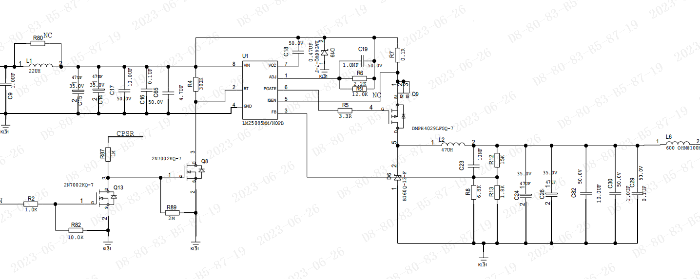
The schematic diagram is as follows, the Rt is changed from 390k to 200k, and the frequency does not change.

Here gives the circuit of LM25085-Q1 according to the customer application.
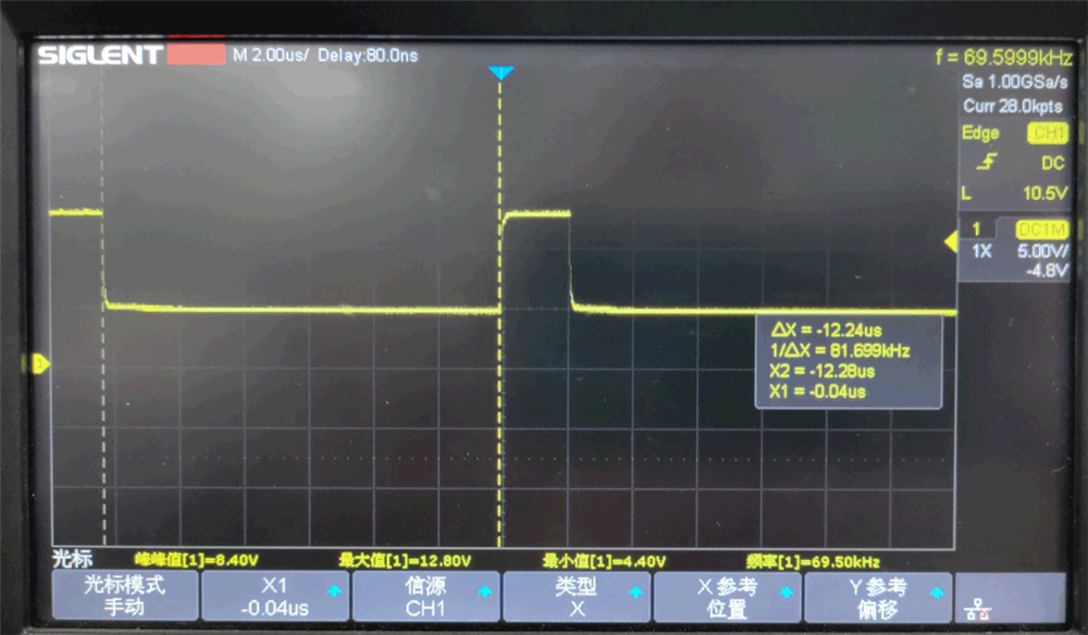
The switch node waveform of these two mission profiles is given below:

1. Input 13V output 10.5V0.75A, working under current-limiting conditions, the gap between the conduction time and the calculated one is large, and changing Rt cannot be adjusted (pay attention the switch node waveform is up-down opposite, the cursor select the turn-on time, which is far from the calculated setting time)
The inductor current and output voltage waveform under this condition is given below:

2. Input 16V output 14.3V0.6A, working under non-current-limiting conditions, the gap between the conduction time and the calculated one is large, and changing Rt cannot be adjusted.
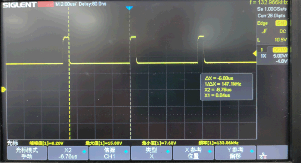
The inductor current and output voltage waveform under this condition is given below:
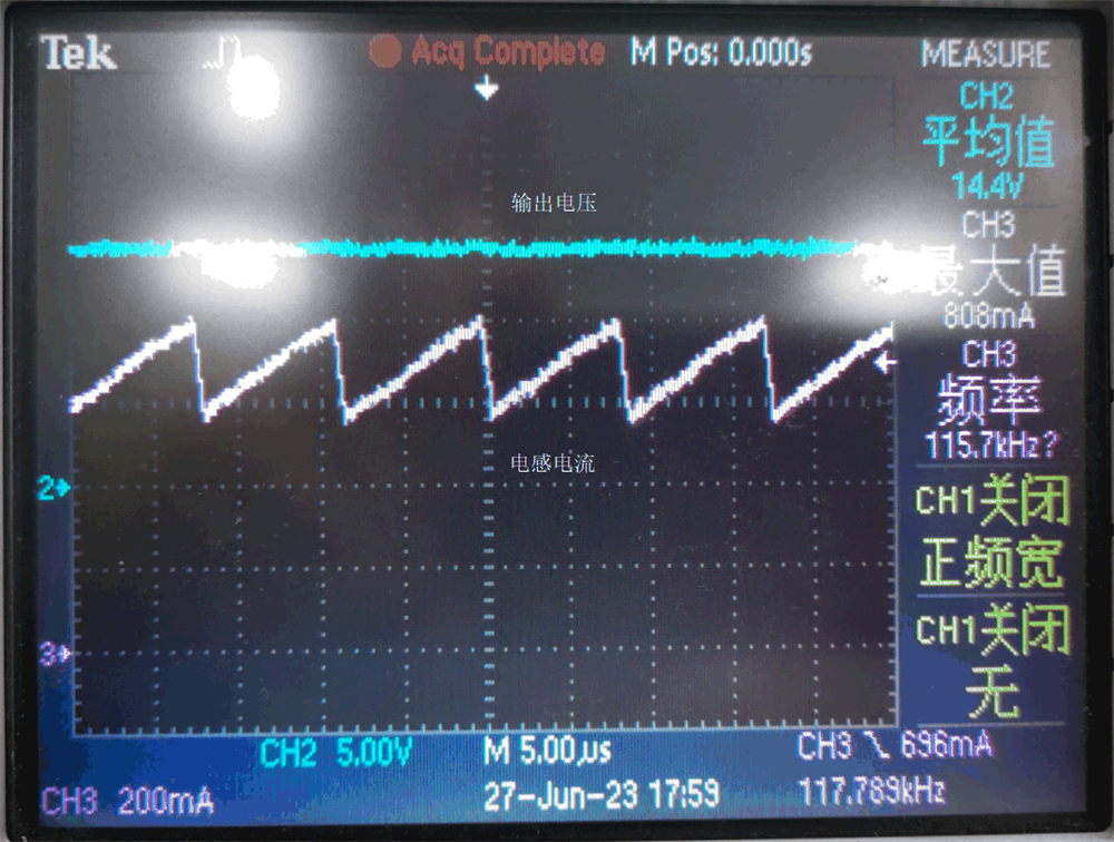
It seems that the chip does not operate at a DCM mode, so I need help for explain the reason for error switching frequency (turn-on time).

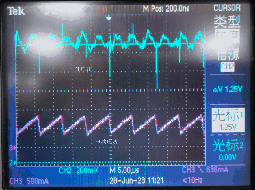
  • With COT topology it would seem that the PFET is triggered on everytime FB falls under a certain threshold (1.25V for this part). Could you check the FB voltage for me and see if the ripple is behaving properly during the two different operations?

    Regards,

    Henry

  • Hi Henry,

    My customer provides the FB waveform of the second mission profile:

    Input 16V output 14.3V0.6A, working under non-current-limiting conditions.

    Thank you.

    Regards

    Matt

  • Hi Matt,

    Thanks for taking the scope shots. This is an interesting case and I will continue examining and get back to you tomorrow.

    Regards,

    Henry

  • Hi Matt,

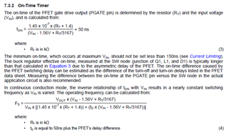
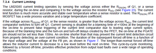
    There may be an issue where the device minimum on time for the PFET at the gate should not be set for less than 150ns. And the current limit circuit is triggering your PFET to shut off prematurely. Maybe carefully increase the current limit and draw current with an electronic load to see if the device still has this abnormal switching frequency issue.


    Regards,

    Henry

  • Hi Henry,

    It seems that the turn-on time of the PFET is set larger than 150ns (3.8us and 2.01us for 390kOhm and 200kOhm), and the current limit circuit is not triggered in case of the mission profile II (the limitation is set as 0.75A).

    However, both mission profile occurs the abnormal switching frequency.

    Can you give other more potential causes to this problem?

    Thank you!

    Regards,

    Matt.

  • Hi Matt,

    I see what you are saying. Thanks for clarifying. I will check back with the team and get back to you next week.

    Thanks for your patience.

    Henry

  • Hi Matt,

    Please check your values using the LM251085 quickstart calculator: https://www.ti.com/tool/LM25085-5085QUICK-CALC. The injected ripple to FB should be in the 50-100mV range.

    If you suspect noise affecting the circuit, please send the PCB layout for review. in particular, the FB node is noise sensitive and the FB trace should be as short as possible (locate the FB resistors very close to the FB pin).

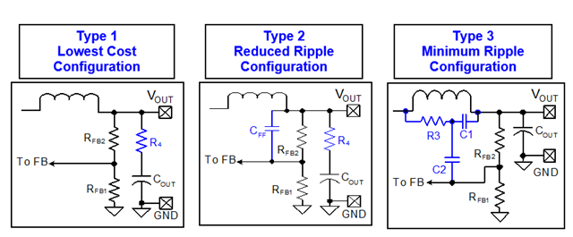
    Upon further examination it seems like the FB ripple waveform is not representative of inductor current. For COT, it is not good practice to place low-ESR ceramics on the output in parallel with your electrolytics because the low ESR will dominate and cause the output ripple to be no longer triangular. I recommend using a type 3 ripple injection network.

    Regards,

    Henry