This thread has been locked.

If you have a related question, please click the "Ask a related question" button in the top right corner. The newly created question will be automatically linked to this question.

BQ76952: Functionality of DFETOFF and CFETOFF with Parallel FET configuration

Part Number: BQ76952
Other Parts Discussed in Thread: BQSTUDIO

Hi,

We're using the BQ76952 in a parallel FET configuration (we have Settings:FET:FET Options - SFET set to 0), and we're noticing strange behavior regarding the CFETOFF and DFETOFF pins.  We're controlling these two pins via a microcontroller and both pins are configured to their alt functions (Settings:Configuration:CFETOFF/DFETOFF Pin Config both set to 0x2).  Individually, these pins both function properly.  If only one of the pins is high, the corresponding FET will indeed be off.  However, in our firmware logic, when switching between charge or discharge mode, all of the charge/discharge circuitry is turned off before enabling the other side, so there will be a brief period where both CFETOFF and DFETOFF are high.  However, this doesn't seem to be the case, and instead when CFETOFF and DFETOFF are both high, the discharge FET seems to stay on.  I understand that in a series configuration, this would be expected behavior in order to protect the discharge FET, but why is this happening in parallel mode?

  • Dear Nathan,

    That sounds odd. If you don't typically use CFETOFF and DFETOFF individually and most of the time it is both at once, you can try setting the Settings:Configuration:DFETOFF Pin Config[Opt4] bit high. When this bit is high, triggering DFETOFF will disable both FETs, and not just one. Are you attempting to do manual control of the FETs or is this just for swapping between charge and discharge modes?

    One other thing worth trying if you can't justify using DFETOFF as BOTHFETOFF would be to try setting SFET high to see if it makes a difference. In all likelihood, it shouldn't make a difference, but it would be worth trying to determine whether its a paralleling issue or not. If neither of these options show any difference, could you share your schematic? It would be helpful to see the hardware setup for the gate drive loop as well  as CFETOFF and DFETOFF.

    Best,

    Asher Nederveld

  • We do want manual control of the FETs from the microcontroller, so BOTHFETOFF doesn't seem viable.  One note I forgot to mention was that the DSG FET only comes on once voltage is applied by the charger.  So, with battery voltage applied, no charger voltage, and both CFETOFF/DFETOFF high, both FETs are indeed disabled.  However, in this same state as soon as a charger voltage is applied, the discharge FET turns on.

  • Dear Nathan,

    Ah, I didn't realize that it only turns on when a charger is applied. This makes me think that it might be a leakage current issue with the hardware. Could you share your setup schematic for the circuit as well and take the following measurements for me when the turn-on occurs:

    1. Voltage at the DSG pin relative to VSS

    2. Voltage across DSG FET

    3. Voltage at CP1 relative to GND

    4. Voltage at the CHG pin

    5. Not really a measurement, but check whether the device is in SLEEP before the charger is attached

    Likewise, if you happen to be interfacing with the device on BQStudio, could you share your .gg file that has the set-up for all your registers?

    Best,

    Asher Nederveld

  • Hi again,

    I'll be able to get those measurements for you later today. As far as the schematic, I won't be able to post them publicly, so is there any way for me to provide relevant sections to you privately?

    Thanks

  • Dear Nathan,

    I sent you a friend request through E2E. If you accept it, you can send me the relevant parts there.

    Best,

    Asher Nederveld

  • Hi,

    I send the schematics to you privately.  Below are the measurements you asked for with the DFETOFF and CFETOFF pins in different states:

    DFETOFF = 3.3V CFETOFF = 3.3V Both = 3.3V
    DSG PIN 44V 45.6V 43.8V
    Across DSG FET 11.5V 0V 0V
    CP1 65V 46.4V 46.4V
    CHG Pin 65V 35.5V 35.5V
    Across CHG FET 0V 0.3V 0.3V
    Battery Voltage 36V 36V 36V
    Charger Voltage 48V 48V 48V

    Looking at these results, it seems that we don't have control of the DSG pin at all.

    Unfortunately we aren't able to use BQ studio on this board and we are programming the BQ over I2C using the microcontroller.  Both the Settings:Configuration:CFETOFF Pin Config and DFETOFF Pin Config are set to 0x2 though, and Settings:FET:FET Options is set to 0x2C.

    Let me know if there are any other relevant registers we should look at the configuration for.

    Thanks

  • Dear Nathan,

    I looked over you schematic and couldn't find anything wrong with it that would produce the results you are seeing. Normally a 22nF capacitor is put between REGIN and BAT- to improve the performance, but that wouldn't cause the issues you are seeing. However, the data you provided has a large amount of oddities with the CP1 and CHG pins. From the data, the battery voltage is 36V and the charger voltage is 48V. However, the CP1 voltage when DFETOFF is enabled is far too high. Its only meant to produce 11V above the BAT pin at most. Even assuming that while charging that the BAT voltage equals the charger voltage, it still falls 7V short. Could you try measuring the BAT pin voltage in these three scenarios as well? If you have DDSG and DCHG enabled to mimic the DSG and CHG signals, it would also be good to see if those pins are reacting properly to DFETOFF and CFETOFF. If they turn off when DFETOFF and CFETOFF are sent, then it will be a hardware issue of some sort pulling the DSG and CHG pins high.

    Based on your data, it seems like there is a correlation between disabling the CHG FET (during both off) and then seeing realistic values for the DSG  and CHG pins versus when it's only DFETOFF. This makes me think that there might be leakage current somewhere.

    Best,
    Asher Nederveld

  • Hi,

    My mistake, the board is using a 48V charger, but I forgot that before it gets to the BQ it's boosted to 54.5V.  The BAT pin is at ~54.1V with DFETOFF high, and CP1 at 65V seems to make more sense with that in mind.

    We also tried disconnecting the DSG pin from any other circuitry and verified that the 43.8V is in fact coming from the BQ itself (while DFETOFF was asserted).  We also tried this with a couple of boards to verify that it wasn't one faulty BQ/Board, this problem existed on all of them.  So I'm not sure if there's a register setting that we're missing?

    Thanks

  • Dear Nathan,

    Ah okay, that makes a bit more sense as to why you were seeing 65V. If the charger wasn't boosted, that would have been a bigger issue. That's intriguing to hear that the pin was by default outputting 43.8V. Have you confirmed that their is continuity between the DFETOFF signal and the BQ chip on the board? On a similar string, could you check the 0x7F FET Status register when both DFETOFF and CFETOFF are asserted to see whether the device thinks that the DSG is asserted?

    The main registers I can think of affecting the DSG FET operations are the CFETOFF/DFETOFF config (but yours seem fine), FET Options, Settings:FET:Chg Pump Control[SF_MODE], and the body diode protection register (which should be disabled since SFET=0). Could you share the code you are using to write to CFETOFF and DFETOFF as well as the parts where it is called? It would be good to know whether you are using the provided TI functions or a custom one.

    When you are using CFETOFF, I noticed the voltage across the CFET is only 0.3V. However, shouldn't it be more than since the battery voltage is 36V and the charger voltage is 54V, leaving a differential voltage of 18V.

    Best,

    Asher Nederveld

  • Hi,

    Yes, we confirmed continuity between DFETOFF and the microcontroller.  

    Looking at the FET Status register, the reported FET statuses accurately reflect the intended state (FET Status reports DSG as 0, but still measuring 43V on the FET gate).  

    We are using our own code to configure the BQ over I2C.  This code was tested and verified on an evaluation board for the BQ where we were able to connect to it via BQStudio after letting the microcontroller configure the device, and BQStudio reported the correct values.  We did also attach leads to one of our board's I2C lines and were able to connect this BQ to BQStudio that way, and again the values looked configured as we intended them to be.

    When using CFETOFF, the voltage across CFET is 0.3V because the charge voltage gets blocked by another FET in our design.  So in a discharge state, only the battery voltage should be across CFET.

    As far as the other registers you mentioned, our configurations are as follows:

    • FET Options: 0x2C
    • Settings:FET:Chg Pump Control: 0x1

    Thanks

  • Dear Nathan,

    Since there is another FET along the CFET path, is there any other circuits that are significant connecting to the DFET path? In a similar vein, does CFETOFF control the other FET you mentioned between the charger and the circuit you have sent me? Due to the registers being correct, it is most likely some form of leakage current in the hardware so any information you could provide on the discharge and charge loops that weren't in the two images you shared with me would be extremely helpful.

    One thing I noticed on the schematic was that used BAT- as GND for almost every connection, but between SRP and SRN you have a GND symbol. I just wanted to double check that BAT- and the GND symbol were connected somewhere on the schematic. This change isn't required, but it is often a good practice to have a capacitor from REGIN to BAT-, typically around 22nF.

    Best
    Asher Nederveld

  • Hi,

    I sent you an additional bit of the schematic in a PM that shows the connection between GND and BAT-.  We do intend to add the 22nF cap as well, though as you mentioned that shouldn't be related to this issue.

    The other FET in the charge path isn't connected to CFETOFF, the rest of the path components get controlled by our microcontroller, so the charge voltage gets blocked much further down the chain.  The discharge path also has an additional blocker between the BQ and the system power bus, and we're able to measure some of the battery voltage on one side of that blocker (only because the BQ DFET 44V) and the charger voltage on the other side.

    Thanks

  • Dear Nathan,

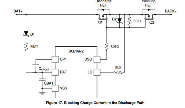
    Where are you connected LD_PACK node on your schematic? Typical parallel FET applications will split the two nodes as LD is used for detecting a load on discharge while PACK is used to detect a charger. Since your two pins are sharing the same node, that might cause leakage issues as the DSG pin is discharged towards the LD pin and not to GND to protect it during turn-off. This is described in section 16.5 of the datasheet. If LD is connected to the charger instead of the discharge, it might cause the leakage issue. I've attached captures from the Parallel Paths with the BQ769x2 Battery Monitor app note to show typical usage of the LD and PACK pins on a parallel application. Could you try adjusting your LD pin to see if this makes a difference?

    Best,

    Asher Nederveld

  • Hi,

    Thanks for pointing this out, disconnecting our LD and PACK pins resolved the issue.

    Thanks a lot for the help!

  • Glad to hear it worked; Best of luck on your project!