This thread has been locked.

If you have a related question, please click the "Ask a related question" button in the top right corner. The newly created question will be automatically linked to this question.

BQ76952: About the ground of bq76952

Part Number: BQ76952
Other Parts Discussed in Thread: TIDA-010208,

Hi TI's experts,

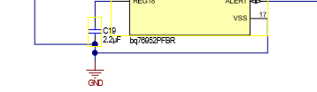
1. When I design the schematic diagram, because the reference ground inside the AFE is B-, and the reference ground of the externally connected MCU circuit is P-. Confused about which ground is referenced to SDA/SCL, B- or P-? If it is B-, does it affect the IIC communication when the current is high? If it is P-, does the reference ground of AFE need to be adjusted to P-?


2. Can the ground of bq76952 be placed at the P- position, that is to say, I place the reference ground near the P- terminal of the sampling resistor. Will this have any effect? Will it affect the sampling of AFE?

  • Dear JH,

    1. I'm slightly confused why you are referencing the MCU to P- instead of B-. Which design are you referencing that has the MCU connected to P- and not B-? In TIDA-010208, our high side reference design, the DVSS pin of the MCU is connected to GND as is the AFE. I would suggest adjusting your design so that the MCU and AFE share the same ground. the GND for SDA/SCL should be B-. If you were to keep the two different GNDs as is, you would see the issues you describe when current goes high. However, the solution would be to set the MCU to B-, and not the AFE to P-.

    2. As for placing the GND of the AFE at P- instead of B-, I would recommend against it. In order for the device to measure properly, the voltage of VC0 must be within 0.5V of the internal GND reference of the device. If the GND is referenced at P-, there is a significant chance that during large currents, the voltage difference between P- and VC0 would be large enough to make the measurement inaccurate.

    Best,

    Asher Nederveld

  • Hi Asher,

    Thank you for your answer.

    Thank you for your answer.
    When I design the schematic diagram, there will be a 0.5mR sampling resistor between B- and P-, and I refer to the bq76952 data sheet document on TI's official website, which is on page 68.
    Also refer to the Demo BQ76952EVM schematic diagram provided by TI. The project name is BMS029B. The ground of the MCU is connected to QGND, which comes from PGND on the AFE. Both places describe that AFE communicates with the outside through IIC, and the ground reference of the external MCU is P-.

  • Dear JH,

    Either option will work in a design. However, connecting MCU GND to P- will cut into the noise margin on the digital signal as the discharge current increases. I would read through this thread here for more info: https://e2e.ti.com/support/power-management-group/power-management/f/power-management-forum/959098/bq76952-ground-rail-voltage-difference

    Once again, you can use either based on your preferences, but I would still recommend connecting the MCU to B- and not P-. One thing you could do if you prefer to connect it to P- is calculate the sense resistance so that the voltage across it is never large enough to distort the digital signals at high currents.

    Best,

    Asher Nederveld

  • Hi Asher,

    I'm evaluating moving the AFE's GND to P-, besides the inaccurate VC0 measurement, are there other considerations to consider? What I think is that the current causes the voltage of the sense resistor to change, which will cause the reference ground of the AFE to change, right?
    What are your considerations, why is it not recommended to move GND to P-?

  • Dear JH,

    The AFE has not been characterized with GND as P-. While there is a chance that it could work, I can't guarantee it as the circuit was designed with the AFE's GND being B-. Certain pins Plus, if you are using low-side driving, connecting the AFE GND to P- will disconnect the AFE from power once the FETs turn-off, rending the circuit unable to function.

    In general, I would recommend connecting the MCU GND to B- rather than connecting the AFE GND to P-. Besides from the many subcircuits that were designed with the assumption that B- is the GND of the AFE, it's best not to try to modify how the SRP and SRN pins should operate as you would be changing SRP from being 0V to SRN being 0, changing the offset of current measurement. Is there a reason you are leaning more to P- rather than B-? There isn't really a drawback to connecting the MCU to B-.

    Best,

    Asher Nederveld

  • Hi Asher,

    It is because the MCU introduces other control chips. If B- is used as the ground, the control signal will fluctuate, so its ground can only choose P-.
    The problem now is that when I was layouting the PCB, due to layout restrictions, the ground B- of the AFE and the ground P- of the MCU were too far away, so I evaluated changing the ground of the AFE to P-.
    1. As you said, if the ground of AFE is changed to P-, it will cause measurement error of VC0 (that is, the voltage of the first battery cell), and at the same time, will the measurement sampling of SRN and SRP be incorrect? According to my understanding , SRN and SRP are not differentially sampled, why is there an impact?
    2. If the ground of AFE is changed to P-, will it cause other effects?

  • Hi JH,

    As Asher stated in the previous posts, the BQ76952 is characterized with VSS referenced to B-, and connecting VSS to P- is not recommended for reasons shared in the linked posts below:

    Please see this thread with respect to SRN/ SRP and VSS connection: (+) BQ76952: Can I connect VSS to SRN instead of SRP - Power management forum - Power management - TI E2E support forums

    Effects of AFE connecting to P- instead of B- have been discussed in this previous post linked above: (+) BQ76952: Ground Rail Voltage Difference - Power management forum - Power management - TI E2E support forums

    If the hypothetical and theoretical answers are not sufficient, and you want the AFE and MCU to share P- GND connection despite the advisory against this, then I recommend creating a circuit with your proposed ground connections and testing it under a variety of your expected conditions.  The BQ76952 was created and tested with certain GND connections in mind, so providing exact details on part performance in this configuration is not possible.  My apologies for any inconvenience, and I hope the resources that have already been provided are sufficient.

    Best,

    Andria

  • Hi Andria,

    When I design the schematic diagram, I evaluate the impact of moving VSS to P-. This is the information I want to know now.
    1. For example, what you said in your reply will lead to changes in VC0 measurement. Can you explain why from the equivalent diagram of the internal pins? I see the equivalent diagram of VC0, there will be a diode between VC0 and VSS, is this the reason? Will the voltage difference generated by the sampling resistor cause the diode to conduct?
    2. For SRN and SRP, my understanding is that these two pins are differential sampling currents. I don't understand why it will affect the current measurement

  • Hi JH,

    As stated in this post ((+) BQ76952: Can I connect VSS to SRN instead of SRP - Power management forum - Power management - TI E2E support forums), placing the VSS connection on the P- side could potentially push SRP and VC0 significantly below VSS.  If the recommend voltage ranges listed in the data sheet for these pins are violated, this will affect the measurements taken using each of these pins, and if the abs max values are violated, the part can be damaged.

    I understand your frustration with being unable to see exactly why the internal workings of the IC give rise to the datasheet specs, but this gets into IC design and confidential information.  The pin equivalent diagrams are useful tools for understanding the general logic of the pins, but they should not be treated as a comprehensive schematic that can be used to calculate acceptable conditions for each pin.  

    Please follow the voltage ranges listed in the datasheet for each pin.

    Best,

    Andria