This thread has been locked.

If you have a related question, please click the "Ask a related question" button in the top right corner. The newly created question will be automatically linked to this question.

LM7480-Q1: LM74800-Q1

Part Number: LM7480-Q1
Other Parts Discussed in Thread: LM74800-Q1,

Hello,

i need your help please...

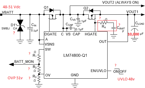
i'm designing a new circuit with LM74800-Q1 (Ideal Diode Controller with inrush current limiting) my inputs are: 

A) input voltage 48-51 Vdc

B) Current pass of 20A

C) i have choose 2 same N channels mosfets with low rds(on) of ~3.5-4.5 milliohms, (30A)

the needs from the circuit are :

1) Minimum forward voltage losses (low rds), with supporting current pass of 20A

2) Reverse Battery Protection

3) Reverse Current Protection

4) Inrush current limiting

5) Overvoltage Protection (above 51Vdc)

6) EN with under voltage protection (below 48Vdc)

also note that i have a Bulk capacitor at the output of 10,000uF, is there any consideration need to be taken about it ?

Please help me to figure out the exact values of the parts to reach those needs... (R1, R2, R3, R4, Cdvdt, D1, ENUVLO)

thanks in advance

  • Hi ilya,

    To set Vin OV threshold at 51V, you will have to select (R1+R2) and R3 such that when Vin is 51V, the voltage seen on the OV pin is  V(UVLOR) = 1.231V.

    Let's say you have chosen (R1+R2)  = 100 kΩ , then you will have to chose R3 around 2.47 kΩ

    If you have a huge output capacitance of 10mF at the output, you will have to select the Cdvdt capacitor appropriately such that the inrush current is acceptable and the operation of FET within SOA during startup. You can use the attached design calculator to select the appropriate dvdt capacitor and FET with suitable SOA for your input voltage and output capacitor. Please go through the training videos in design calculator before using it. 

    7217.INRUSH_FET_SOA Margin Calculator.XLSX

    Since your operating voltage is higher and if the dvdt capacitor (Cdvdt) selected is higher (> 100nF) we recommend to use an additional circuit (PNP transistor, diode and 1k resistance) to discharge the Cdvdt locally (within the pnp transistor) as shown in the dotted box below. if this circuit is no used the Cdvdt capacitor will discharge in the LM7480-Q1 IC and can damage it. 

  • Hi Praveen

    thank for your reply, after searching a bit i have found that the best part for my needs would be LM74810 which is almost the same.

    if i add the additional circuit (PNP transistor, diode and 1k resistance) as you suggested, do i also need to add a series resistor between HGATE and the MOSFET GARE, and if yes what would be the best part ?

    what about the UVLO pin (below 48V) ?

    what about D1 ?

  • Hi ilya,

    If there are multiple FETs in parallel, a series resistance of around 4Ω - 10Ω can be used in between HGATE of the controller and gate of each FET. These resistors help dampen out oscillations between FET parasitic gate capacitances and  path/FET lead inductances. In case you only have a single FET, the series resistor will not be required. 

    The device can withstand a voltage of 65V across EN/UVLO to GND. So, 48V across EN/UVLO to GND should not be a problem.


    You need to select D1 such that the break down voltage of the TVS is 51V and the maximum clamping voltage of the TVS during all transients is  less than 65V. 

  • Hi Praveen

    thank for your reply, please tell me about the D2 Schottky protection diode on the output (voltage, current,...) because in the datasheet there is no information about it what is recommended...

  • Hi Ilya,

    When the external MOSFETs turn OFF during the conditions such as overvoltage cut-off, reverse current blocking, EN/UVLO causing an interruption of the current flow, the input line inductance generates a positive voltage spike on the input and output inductance generates a negative voltage spike on the output.

    The peak amplitude of voltage spikes (transients) depends on the value of inductance in series to the input or output of the device. These transients can exceed the Absolute Maximum Ratings of the device if steps are not taken to address the issue.

    The OUT pin is rated for only -0.3V on the negative side. So, you can consider using a Schottky diode across the output and GND to absorb negative spikes at the output. This is generally required in case you have inductance at the output in the form of inductor or long cable. 

  • Hi Praveen

    thank for your fast reply, i understand but please tell me what would be the best Schottky parameters for that case ?

  • Hi Ilya,

    The Schottky diode selected should be such that its should have a forward voltage drop of  less than 0.8V for the maximum current that can flow through the FETs before the FETs are turned OFF due to EN low or any fault condition. 

  • Hi Praveen

    ok got it, but i still don't know what to choose for the D1 ( TVS input) in the datasheet they give an option to 24V input with 2 TVS but there is no option for 48V TVS, can you help me with this ?

  • Hi Ilya,

    We are very well aware of the transients in 12V and 24V automotive battery systems. So, we were able to provide suggestions for input TVS. For TVS selection on 48V rail you can follow the below guidelines,

    • The breakdown voltage of the TVS has to be greater than the maximum DC voltage that can be applied at the input.
    • The maximum clamping voltage by the TVS during transients has to be within the device Absolute Maximum Rating
    • While clamping for negative voltage transients, the FET Vds rating needs to be taken into consideration. The FET vds rating should be greater than the Max Clamping voltage  on the negative side + the maximum positive voltage on the output that is possible just before the negative transient is applied. 
  • Hi Praveen

    this is the reason that i asked because there is no such part with these parameters...

    the nominal input voltage is 48-53 V and the part limit is 65V so the parameters goes beyond

  • Hi Ilya,

    You may have to consider using a high power TVS which will have a lower clamping voltage. The device ab max rating is 70V , so you can consider the max clamping voltage to be below 70V (not 65V).  Also, you need to calculate the clamping voltage of the TVS for the current flowing into it during the transient event. This can be calculated generally using the Automotive transient parameters provided like peak voltage and input impedance.

  • Hi Praveen

    thank you very much for your help, can you please send me your email i would to send you the schematic for you to check...

  • Hi Ilya,

    Please accept my friend request and share the schematic in private chat. I can share my comments there. 

  • Hi Ilya,

    Reviewed and shared my comments on the schematic is private chat. 

  • Hi Praveen

    yes i see thank you very much i have sent you the updated schematic with a new question, please check...

  • Hi Ilya,

    Shared my comments on the updated schematic in private chat. 

  • Hi Praveen

    the closest value for 400nF is 390nF and 470nF, what would be better to use for the charge pump capacitor ?

  • Hi Ilya,

    The charge pump capacitance has to be >10x (4x10nF). So, you can consider using 470nF.