This thread has been locked.

If you have a related question, please click the "Ask a related question" button in the top right corner. The newly created question will be automatically linked to this question.

LM3481: MOSFET Heating

Part Number: LM3481

Hi Team,

I am using the LM3481MMX/NOPB in a SEPIC mode configured for the following values and got the board cleared and approved in a previous thread:

e2e.ti.com/.../lm3481-schematic-review

Vin: 21 to 29.6V
Vout:24V
Iout:1 A

Inductor used: Sumida 0624CDMCCDS-220MC (22uH/ Isat=3.2A)

For the switching mosfet, we used a CSD18511Q5AT and observed that for higher voltages and at NO-LOAD condition, the MOSFET heated up to about 100 deg.C at around 25V. We did not notice this at first and observed it after we did a load test at 1A and ended up damaging the MOSFET and observed the temperature rise after replacing it. Checked the switching frequency at the gate and this never changes. Also at around 22.6V and NO-LOAD the board started drawing about 50mA and as the voltage kept increasing it spiked up to about 200mA from the supply.
What could be the possible issue for this amount of heating and drawing current at NO-LOAD? Also please suggest possible changes and diagnosis. 

  • HI Noel,

    not sure if I got all the details right - let me summarize

    - the issue shows up at no load

    - you observed it after testing with 1A - this is not no load

    - so is this issue at the any load condition with higher voltages.

    - operation with lower voltages is OK - independent from the load condition

    Is the output voltage still stable?

    Can you measure the Switch node and the Gate signal of the MOSFET and share it here.

    Note: even at now load there will be some current consumption for the controller and the MOSFET switching.

    Best regards,

     Stefan

  • 1.This happens at NO LOAD (MOSFET went up to a 100 deg.C)

    2. We observed it after we damaged a MOSFET in a loaded condition. But also showed up during no load

    3.This happens at LOAD and NO-LOAD condition. Sorry to confuse you.
    Operation at lower voltage and NO LOAD is fine. No heating observed. But at NO LOAD and higher voltages it burns at 100 deg.C

    4.Yes the output regulation (both Line and Load regulation) is amazing. Very stable at 24V.

    5.I do not have the setup right now. I will share a photo ASAP.

    6.Even at no load does it consume 200mA? Im assuming this is a very high draw at no load and higher input voltage.
    Lower input voltages and NO LOAD does not draw much (around 10mA)

  • Hi Noel,

    right, if 200mA @ 25 V is burned at the MOSFET this will give 5W - so to much of the MOSFET.

    Just check the MOSFET again you are using: on a SEPIC the MOSFET see the sum of input and output voltage + ~ 55V

    The used CSD18511Q5AT has a rating of 40V ....

    If selecting another MSOFET please consider a margin if at least 20% so 70V or higher.

    Best regards,

     Stefan

  • Ok git it. Made the changes.

    Replaced the current MOSFET with a V_DS=80V and I_D=200A MOSFET. 

    NO-LOAD: The MOSFET is no more heating at no load and higher voltages.

    ON-LOAD: The mosfet heats to about 109deg.C at a load of 1A and maximum Vin(29.6V)

  • HI Noel,

    Is the output voltage still stable?

    Can you measure the Switch node and the Gate signal of the MOSFET and share it here.

    Best regards,

     Stefan

  • Yes the output voltage is still stable. 


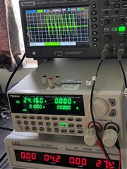
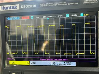
    The yellow one is the switching node and the green one is the MOSFET gate signal.


  • Hi Noel,
    please add the condition for this measurement:

    • input voltage 
    • output voltage
    • load current

    Best regards,

     Stefan

  • input: Vin_min=21V Vin_max=29.6V
    Output: Vout= 24V Iout=1A

  • Hi Noel,

    the waveform does look like it is in DCM mode which should not be the case for the setting you have shown above.

    So something does not seem to match with your hardware setup.

    You can use the power state designer 

    POWERSTAGE-DESIGNER Design tool | TI.com

    to further evaluate the hardware and cross check the signals on your hardware against the one to be expected (shown in the power stage designer)

    Best regards,

     Stefan

  • Hi Stefan,

    Sorry for the long delay in response. 


    As you can see the output is in regulation but the MOSFET is still in an off state with no voltage at the gate terminal. How is the regulation being achieved in this condition? 
    I am assuming that the body diode of the mosfet is what conducts the load current and hence the heating. I do not understand why this is working in DCM.  Sharing you the Gerber and the Schematic again on private chat. Please check and let me know if there's any error in that.

    Thanks and regards

  • Hi Noel,

    i am not sure on what and how i need to read the information shown in the picture.

    Can you add some details?

    (The body diode of the MOSFET should not get conducting and without switching there will not be an output voltage on a SEPIC.)

    Best regards, 

     Stefan

  • Hi,

    So the oscilloscope reading shown in the image is the gate volatge w.r.t ground. The DR pin is not providing any voltage (300mV range) and this means that the MOSFET itself is off, I even checked the voltage at Vds to confirm that the MOSFET is off. Yet the regulation is being achieved at the output for the required voltage range (21V to 29.6V input that i require) .

    On adding an output load of 0.1A the MOSFET starts heating up to almost a 100Deg.C as mentioned earleir in the post. The regulation is still achieved in this condition too but i am not able to achieve the load of 1A (which is my requirement) due to insane levels of mosfet heating on LOAD. I really cannot understand why this is happening.

    Please look into the information provided and suggest possible solutions.

    Thanks and Regards

  • Hi Noel,

    thanks for the details.

    But i just can repeat my previous statement: If the MOSFET is not switching there could not be any output voltage. There is no DC path there.

    So either the measurement fools you or something is damaged and there is another path where the current can flow.

    Can you check your measurements and your circuit for that?

    Best regards,

     Stefan

  • Hello again Stefan,

    I am attaching the Power stage designer results on our private chat. Please take a look at this and let me know if all looks good.


    We are still facing the issue of MOSFET overheating. 

  • Hi Noel,

    Stefan is out of office for the next two days, so he will reply to your private message once he is back.

    Thank you for your patience.

    BR,

    Haroon

  • Ok thanks for letting me know!
    Will wait

  • Hi Noel,

    unfortunately the Power stage designer does not support compensation for the SEPIC topology. Therefore the results are different.

    I am not sure about the current situation on your side now:

    Are you still seeing the MOSFET gets heated up without switching? Or has this changed now.

    Best regards,

     Stefan

  • That has changed. The MOSFET is switching well on load. But still heating to insane amount (Almost 95-100 deg.C)

    The current flow across the sense resistor is also right.

    Mosfet that we currently use is an 80V mosfet 

    What can we do about the heating? do you have any suggestions to solve this issue?

    Also, i hand calculated the coupled inductor values (As mentioned in AN-1484 Designing A SEPIC Converter (Rev. E)) required at 520kHz, 29V vin and 1A load. The value came out to be 24.8uH for my system, but inputting the same values on the power designer for coupled inductors gave me a value of 48uH. So which value should i be using? It  got a  little confusing for me. 

  • Hi Noel,

    so if the MOSFET heats up to 95 Degree it is a delta of ~ 70 Degree

    Assuming you have the AON6144 and a mounting area as given in the datasheet index A, the power loss should be around 1.75W

    Please check if this would match with the math as shown here:
    https://www.ti.com/seclit/ml/slup270/slup270.pdf (section MOSFET selection)

    Best regards,

     Stefan

  • The MOSFET Currently used is a VISHAY SIR104LDP-T1-RE3 . 

    fsw=520kHz
    Io(max)=1A
    Vo=24V
    Vin=21V to 29.4V

    Acoording to my calculations  the power dissipation is well below 1W

    Also, i hand calculated the coupled inductor values (As mentioned in AN-1484 Designing A SEPIC Converter (Rev. E)) required at 520kHz, 29V vin and 1A load. The value came out to be 24.8uH for my system, but inputting the same values on the power designer for coupled inductors gave me a value of 48uH. So which value should i be using? It  got a  little confusing for me. 

    I'd appreciate it if you can give a suggestion to what i should do for this problem that i face too.


  • Hi Noel,

    In this case something is not as it should be - so checking the math against measured data, with:

     - that the MOSFET on time and off time are as you have assumed

     - the rise and fall time on the MOSFET gate is as assumed.

     - the Gate voltage level is right (high and low)

     - are there oscillations / ringing at the Switch node

    From your previous layout I have seen that you have used single inductors - is this right.

    From the data above it looks like more you have coupled inductor selected in power stage designer (what did you use for the Diode Voltage drop and for the inductor ripple).

    Basically the power stage designer uses a more accurate mathematical model - the used formula can be found here: https://www.ti.com/seclit/ug/slyu036/slyu036.pdf

    Best regards,

     Stefan

  • From your previous layout I have seen that you have used single inductors - is this right.

    From the data above it looks like more you have coupled inductor selected in power stage designer

    Yes, but we want to design a new board using coupled inductors.


    Basically the power stage designer uses a more accurate mathematical model - the used formula can be found here: https://www.ti.com/seclit/ug/slyu036/slyu036.pdf

    Thank you so much. I will refer this.

     - are there oscillations / ringing at the Switch node

    I will check and let you know. Will send it as soon as i can

  • Hi again Stefan

    So we went ahead with the coupled inductor plan for the same configurations:
    Vin: 21V to 29.4V
    Vout:24V / 1A

    I am sharing the new schematic and board design in the private chat. Please take a look at this

    The board is regulating well at 24V± 2% . Again like the dual inductor design that we previously did, the board is heating as follows

    Vin:28.7V (For below values)

    At a load of 50mA, the mosfet is at +6 deg.C above ambient (33 deg.C)
    At a load of 100mA,  the mosfet is at +14 deg.C above ambient (33 deg.C)
    At a load of 500mA,  the mosfet is at +31 deg.C above ambient (33 deg.C) 
    At a load of 1A,  the mosfet is at +40 deg.C above ambient (33 deg.C)

    The IC ,when a load of 1A is applied goes upto +44 deg.C above ambient (33 deg.C)

    Are these values normal for a load of 1A?

    Even at lower Vin (22.4V) than the output voltage (24V), similar temperatures are observed.
    We believe these temperature values are really high and are not able to figure out why this is happening. Please suggest possible solutions. 

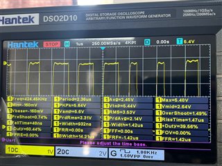
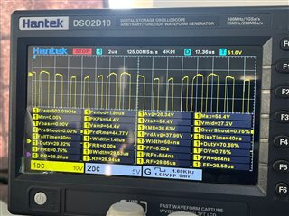
    The MOSFET_Gate has been observed as follows on the oscilloscope at 1A load:


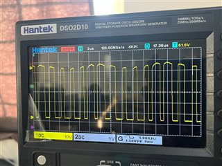
    Figures below shows the MOSFET_Vds measured on oscilloscope at 1A load:


  • Hello Noel Binny Abraham,

    The thermal behavior of the MOSFET and IC is heavily influenced by the layout and the switching frequency. So some heating is normal.

    The high level of the DS seem to oscillate somehow. Can you please check the output voltage? This might increase the temperature as well.

    Best regards,
    Brigitte

  • So at a load of 1A and 520kHz a deltaT of 40 eeg. C is expected? I will share the gerber with you in private chat. Please take a look at it.

    The output voltage is stable at 24V?

    This might increase the temperature as well

    Can you please elaborate 

  • Hello Noel Binny Abraham,

    How efficient is your converter at 1A output? A rule of thumb is that half of the dissipation is in the switches, so you can estimate the power dissipation the MOSFET needs to handle.

    Best regards,
    Brigitte

  • The converter at 1A load/24V vout is 80% efficient. Is this expected?
     

    The mosfet we use is SiR104LDP

  • Hello Noel,

    According to the picture above, your power supply board is very small. I expect that the MOSFET temperature is almost linearly rising with load. If this is correct, the MOSFET does not have enough heat sink on the board and you might need to add a heat sink or increase the board size.

    Best regards,
    Brigitte

  • So adding a heatsink or going for a board with better planes and 2 ounce should help with this right?


    I expect that the MOSFET temperature is almost linearly rising with load

    Actually up until a 0.5A load this is true and the mosfet does not heat much, but right at 0.6 or 0.7A and above until 1A the mosfet shoots upto 40deg.C above ambient. So i wouldn't say the temp rise is linear.

  • Hello Noel,

    It is possible that the converter does not switch permanently at the low output currents and that the temperature rises when it switches with the set swtiching frequency, but you would need to check the switch node to proof this.

    Normally more space and 2 ounce copper on top and bottom helps to keem MOSFETs cooler. I have seen in the meantime as well that several designers of boards are adding a lot of vias to the other side of the board below the MOSFETs and add a heatsink on the other side as heat flow out of the thermal pad on the bottom is better than to the top of the package.

    Best regards,
    Brigitte