Other Parts Discussed in Thread: LM74900-Q1, LM74502-Q1
Hello,
We have the need for an input protection device that can tolerate the tests outlined in ISO21780 (As well as ISO16750 in a different configuration). Our device also needs inrush limiting, reverse polarity protection, low quiescent draw < 100uA, and AEC approval. The ISO test I am currently concerned with involves 70volts for 40ms. We also require to be fully operable @ 60v.
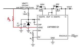
As this 70v test is above the recommended operating voltage for nearly all of the Ideal diode/ORing controller type devices I am looking at the common source configuration. Looking at the LM7480-Q1 datasheet, Figure 10-25 I wonder what the quiescent current draw at nominal 48volts Vbatt would be when the device is disabled EN/UVLO=0v. D1 would give some reverse leakage current. The draw through R1 to the VS pin, I imagine to be similar to common drain configuration ~3uA, is this assumption correct ? If operating with the switch in "OV Cut-Off" mode then R2 and R3 will provide >> 100uA draw. Is it not possible to use the internal switch between the VSNS and SW pins in common source configuration to remove the R2 and R3 current draw when disabled ?
What other devices in the "Ideal diode/ORing controllers" class support common source configuration ?
In this thread Praveen GD mentions an upcoming device "We do have a device which will be released in a couple of months which can work in CS topology and also has over current and short circuit protection." We have an NDA in place, can you share details of this device ?
Many thanks.