A related question is a question created from another question. When the related question is created, it will be automatically linked to the original question.
If you have a related question, please click the "Ask a related question" button in the top right corner. The newly created question will be automatically linked to this question.
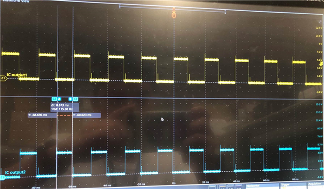
UCC28089: Two 50% PWM signal (+/-180 degree) with manual dead time control
Absolutely. This devices is designed to provide complementary signal (180 degrees shifted) with a max duty cycle of 50% each and with a programmable dead time. To program switching frequency and dead time, use pin CT and DIS. Please refer to pg. 5 and pg. 6 to design those parameters.
If you have any further questions, let me know replying to this thread.
Use 1st order equations showed in pg. 7. Some considerations:
-Tdischarge is the dead time between driver signals (OUTA and OUTB).
-Oscillator frequency fosc is twice switching frequency fs.
Parameters:
fs=60Hz; fosc=120Hz; Tdischarge=(0.03)*(1/120Hz)
Equations:
1.36*Rb*Ct=Tdischarge
5.9/[(Ra+8*Rb)*Ct]=fosc
You can start setting Ra value and then calculate Rb and Ct values. One example for your case:
Ct=200pF; Rb=920ohm; Ra=238.5Kohm
Please, take into consideration that these values are within the range of +/-20% of the real values. Measuring the charge and discharge time at the SYNC pin is recommended to verify them.
If you have any further questions, let me know replying to this thread.