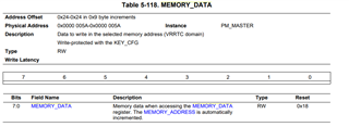
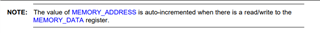
I want to write a data to the specified memory, which will use MEMORY_ ADDRESS and MEMORY_ DATA registers. MEMORY_ ADDRESS is an 8-bit word register used to write addresses to memory, the first 6 MSBs of the MEMORY_ADDRESS register define which sequence word to access (there are 64 sequences, as shown in the MSB Address column of Figures 5-24 below), and the last 2 LSBs define which word to access (as shown in Figures 5-24 below, MSG-M, MSG_L, Delay, Next Address). The data to be written in the memory which is addressed by the MEMORY_ADDRESS register is provided by MEMEORY_ DATA register. And every time write/read MEMORY_DATA register, the value of MEMORY_ADDRESS will increase.
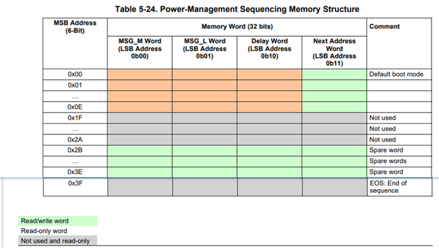
Now I want to write four data to a specified sequence. From charts 5-24 below, we can see that these four data memory addresses (MEMORY_ADDRESS) are adjacent, and TPS65930 supports IIC burst write access. Therefore, I can input all four data at once after writing the device address and register address, instead of writing the device address and register address each time before writing a data. For example, if I want to write four data 21, E, 32, and 2E to a sequence with sequence address 2B (101011), first I will write them in MEMORY_ Write memory address 10101100 in the ADDESS register, and then I start writing MEMORY_ Write data 21, E, 32, 2E in the DATA register
This is the order in which I read the data:
Because every time I write/read MEMORY_ DATA , the values of the MEMORY_ADDRESS register will automatically increase. So after writing the four MEMORY_DATA register data, the value of MEMORY_ADDRESS has automatically increased, so the value of the MEMORY_ADDRESS register is written as 10101100 at first, and then start read data from the DATA register.
The above is how I write and read the order of the MEMORY_DATA registers. But when I finished writing this data, when I read it, I found that the data I read was not consistent with the data I wrote. The data I read was 0, 0, 0, 3F, which is the default value corresponding to these memory addresses. Alternatively, I can assume that I did not write successfully, or that I read data from other memory locations.
Can you help me confirm that the logic of the MEMORY_DATA register that I write or read are correct or wrong? If correct, what caused me to write MEMORY_DATA register inconsistent with what was read?