This thread has been locked.

If you have a related question, please click the "Ask a related question" button in the top right corner. The newly created question will be automatically linked to this question.

UCC28251: OUTA has drive signal when EN pin is lower than 1.5V

Part Number: UCC28251
Other Parts Discussed in Thread: UCC27200, , UCC28521

Hi team,

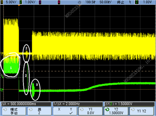
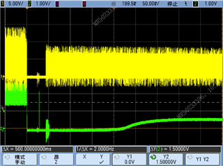
Customer design UCC28251 and UCC27200 like schematics shown. And customer found that when EN pin of UCC28251 is lower than 1.5V, the output of UCC28251 still output drive signal. Could you pls help to comment on it? The green waveform is EN and the yellow waveform is the output signal of UCC28251.

half-bridge.pdf

Thanks!

Rayna

  • Hello,

    I am reviewing your inquiry and will get back to you shortly.

    Regards,

  • Hello,

    Could you label the scope plot waveform for me?

    Regards

  • Hi Mike,

    I mentioned that the green waveform is EN and the yellow waveform is the output signal of UCC28251.

    Rayna

  • Hello,

    I am reviewing your inquiry and will get back to you shortly.

    Regards,

  • Hello,

    I am colored blind and have troubles distinguishing between yellow and green.  That is why I asked you to label the waveforms.

    Interesting fact.  1 in 4 males are colored blind and 1 in 10 women are colored blind.

    After studying these waveforms further.  I can see that one is EN and the other waveform is the OUT.  The lower channel on the plot looks like enable and the other looks like out.  Could you tell me which output this is?

    The enable pin looks very noisy.  Did you take directly across the UCC28521? 

    Regards,

  • Hi Mike,

    Sorry about it.

    The upper waveform is the waveform on OUTA pin. And yes, the lower EN waveform is taken directly on EN pin. 

    Thanks!

    Rayna

  • Hi Mike,

    Customer want to learn the root cause why when EN is lower than 1.5V, the chip is still enabled.  hope you could share some comments here.

    Thanks!

    Rayna

  • Hello,

    I am reviewing your inquiry and will get back to you shortly.

    Regards,

  • Hello,

    I have a few questions about this waveform and recommendations.

    Please note I number the wave form in regards to the questions and recommendations.

    1. Why does the enable pin have over 1 V of high frequency noise on it before it goes low?

       a.) This should not be there and could indicate that your design has a layout issue.

       b.) The data sheet give layout guidelines and a example that the customer can use for a reference and compare it there layout and adjust as necessary.  


    2.  There is noise on the enable pin and Out A during circled interval 2.

         a.) I have see issues where VDD and VREF noise could cause the IC to misbehave as well.

         b.) I would retake the waveforms and look at VDD and VREF as well.

         c.) If you have excessive VDD noise that can generally be resolved with a low pass filter.  22 ohm in series with the VDD capacitors and the aux supply            would help reduce that noise.

         d.) The VDD high frequency bypass capacitors need to be as close to the the VDD and ground pin as possible.

              >Long traces act as antennas and couple noise into the design. 

         d.) If there is noise on VDD that could couple to VREF.

         c.) To reduce VREF noise having the VREF capacitor as close to the VREF pin and IC ground as possible will help reduce noise.

    3.  Time interval 3 high frequency noise going about 600 mV below ground.  If a pin is pulled more than 300 mV below ground it can cause issue with the devices internal isolation and cause the device to misbehave.

         a.) To resolve this issue can generally be resolved by a Schottky diode between ground and the effective pin.  once again having the trace with need to be as short as possible.

    Regards,