This thread has been locked.

If you have a related question, please click the "Ask a related question" button in the top right corner. The newly created question will be automatically linked to this question.

TPS61023DRLR (Observed 3.8V output instead of 5V)

Other Parts Discussed in Thread: TPS61033, TPS610333

Hi,

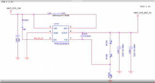
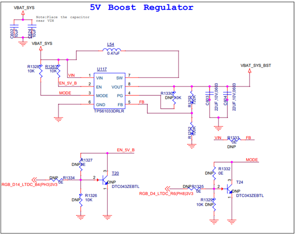
We are using TPS61023DRLR Boost regulator in one of our design. Below is the design requirement.

Vin = 2.7V to 4.2V

Vout : 5V

Max Vout current : 1.5A.

Regulator part Number : TPS61023DRLR

Inductor part Number : SRP4020TA-1R0M

issue Description : Observed 3.8V output instead of 5V

As per the datasheet recommendation; We should get the 5V output voltage for the below design . But we are getting 3.8V instead of 5V.

Kindly let us know; How we can resolve this issue and let me know your suggestion.

  • More Observation on the above circuit.

    Mounted above circuit in 3 General Purpose PCB.  Below are the Observation.

    PCB 1 & PCB 2 :All the impedance were proper; Before Powering ON . After Power ON observed that Pin pin4 & Pin 5 Shorted and Pin 4 & Pin 3 shorted.

    PCB 3 : All the impedance were proper; Before Powering ON. After Power ON observed 5V at the output and after sometime observed Pin pin4 & Pin 5 Shorted and Pin 4 & Pin 3 shorted.

    Pls let me know, How we can resolve this issue. 

  • Hi Suhan,

    About your schematic:

    The feedforward capacitor C623 is way bigger than any design we've ever done before. We recommend calculating the loop stability before making the design. From my rule of thumb, the capacitance should not exceed 10pF for your working condition.

    SLVC803 Calculation tool | TI.com

    Multimeters cannot measure impedance correctly when power is applied so I'm curious about how you measured the impedance with power on. Please give me the waveform of Vin ,Vout ,SW pin, inductor current IL if you would like to debug the device.

    Best Regards,

    Travis

  • Dear Travis,

    We have not mounted C623 during our testing and We have not measured the impedance after the power ON.

    Below Step we have followed.

    Step 1 : Measure the impedance before the power ON .

    Step 2: Powered ON the device and measured the output voltage & Below is the observation.

                 PCB 1 : 3.7V ; PCB 2 : 5V ( after some time 0V) ; PCB 3 : 1.6V

    Step 3 : Turned off the device and measured the impedance of all the PIN w.r.t. GND and Observed 0E to 15E.

    Multiple customer reported similar issue in TPS61023DRLR Boost regulator.


    We are not seen any preferred  solution in TI E2E. Pls let me know the preferred solution for this issue.

     Since we are in Gerber release stage; We are also ready to change the boost regulator part. Pls suggest the alternate boost regulator for this part.

    https://e2e.ti.com/support/power-management-group/power-management/f/power-management-forum/210090/tps61030-internally-shorting

    https://e2e.ti.com/support/power-management-group/power-management/f/power-management-forum/949680/tps61023-tps61023drlr

    https://e2e.ti.com/support/power-management-group/power-management/f/power-management-forum/887079/tps61023-tps61023-output-voltage-drops-during-load


  • Hi Suhan,

    1. Most power supply have output discharge function when the output is not open, which will make multimeters detect a short on the boost input. Please confirm whether you have physically disconnected the supply & load (closing the supply is not enough) when measuring impedence.

    2. If the supply & e-load is disconnected correctly and the short persists, then the lower switch is damaged (most likely caused by poor layout). You can send  your layout so that I can check it.

    If you would like to switch to another device, we recommend TPS61033.

    Best Regards,

    Travis

  • We have not connected any Load during our testing. Is it recommended to connect Minimum load to the Output?

    Layout file attcahed.

  • Hi Suhan,

    It's recommend to disconnect the power supply physically  (closing the supply is not enough) during the test.

    About the layout:

    I can't see how you connected the GND plane. But obviously the output capacitor (which is critical for boost device) is not carefully wired. The layout example aims to reduce the parasite inductance of the output power path , so it's not recommended to use any vias or long path on the output decouple path:

    Parasite inductance on the output path will induce a bigger voltage spike on SW pin and affect reliability.

    For more detailed info of layout.

    https://www.ti.com/lit/an/slvaes4/slvaes4.pdf?ts=1692772366311&ref_url=https%253A%252F%252Fwww.ti.com%252Fproduct%252FTPS61022

    Also, why is your layout mirrored.

    Best Regards,

    Travis

  • It's recommend to disconnect the power supply physically  (closing the supply is not enough) during the test.

    Could you pls elaborate on the above point.

    Since multiple customer reported same issue in actual PCB also; I am quite unhappy to go with tps61023drlr part.

    We have finalized one more new part (TPS61033DRLR )and made the compatible design for TPS61033DRLR & TPS610333DRLR.


    Schematic attached. Could you pls review the same and let me know your feedback n the same.


    Boost Regulator part : TPS61033DRLR / TPS610333DRLR

    Inductor Part : XGL4020-471MEC

    Supply Input Voltage : 2.7V to 4.2V

    Output Voltage : 5V

    Output Current : Max 1A


  • Hi Suhan,

    About the test:

    About other customers:

    Those issues, along with your low side switch damage, are typical problems generated by poor layout. Their totally untrained PCB layout is not likely to work with any ICs.

    About TPS61033:

    1. R1328,R1263 are not necessary

    2. For TPS61033, you can connect FB to Vout to save the voltage divider

    3. For TPS610333, this device only supports 5V fix output. You need to connect FB to Vout.

    4. Layout problems exists for all Boost devices, please also optimize your layout with TPS61033 family

    Best Regards,

    Travis