Hello to the TI support community!
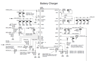
The following is a kind request for a quick review of the schematic and layout and a sanity check of the design decisions.
The charger can be configured for 1S/2S/3S operation with 9V to 15V input voltages and a maximum of 3A input current (USB-C PD input negotiated upstream).
The battery pack is connected with around 5cm of cabling to the board connector which is near the charging circuitry connected with a wide plane. A fuel gauge measures the battery temperature and current. 
1. Was there at any point a benefit in adding a small series resistance to the bootstrap capacitors for EMI considerations (any testing done on previous EVMs)? And if so, is there a recommended value?
2. Given the short battery wiring and the added 47nF capacitor on BATP, should there be any issues with hotplugs? I understand that the 5usec time constant (with 100R series) is there to delay the startup of the SHIP FET such that any other capacitances can be charged, is this faulty reasoning?
3. The JEITA charging profile will be implemented in software by adjusting the fast charge current register (as the fuel gauge reads the temperature). Is it sufficient if TS pin is tied low to stop charging until any software takes control and sets TS_IGNORE? Also, during production, before software is loaded, are there any caveats in injecting a voltage into TS to trick the charger into thinking a thermistor is attached and test the functionality (gated by REGN perhaps)?
Layout: 
The bootstrap capacitors are placed on the bottom layer of the board. The 2nd layer is solid GND and the distance between layer 1 and 2 is 0.14mm with a Dk of 4.2. Total board has 4 layers with 1.55mm thickness.
4. On this particular board, there are some other sensitive components on it and there was a concern in dropping the switching node through the entire board two times (as in EVM). The high dv/dt of the switching node was considered to be more easily managed and that is why only the bootstrap capacitors are on the bottom side (so the high di/dt of the switch node is maintained on the top layer). Is this a decent compromise or are my assumptions incorrect?
5. There were references to a previous EVM that had issues due to vias in the loop of the HF capacitors (on SYS/PMID). Given the above implementation, the stackup and the design constraints, would this layout, at least by comparison with the old EVM, potentially perform better? Note that the main return pin of the charger for the power stage is tied with multiple vias spread on both sides to minimize at least half of the loop inductance associated with the HF loops.
6. If there are any other notes about the layout that I did not ask about, but consider are important, please mention them.
Thank you and Best Regards,
Filip.
-
Ask a related question
What is a related question?A related question is a question created from another question. When the related question is created, it will be automatically linked to the original question.


