This thread has been locked.

If you have a related question, please click the "Ask a related question" button in the top right corner. The newly created question will be automatically linked to this question.

LM5148: Power management forum

Part Number: LM5148
Other Parts Discussed in Thread: LM25149-Q1EVM-2100, LM5149-Q1, LM5149-Q1EVM-400


Hello,

I am currently in the process of constructing a buck converter with the following specifications:

Input Voltage: 15-80V

Output Voltage: 12.51V

Output Current: 10A (Maximum)

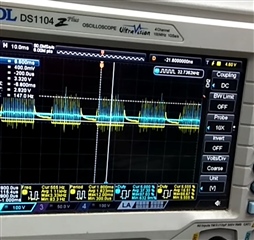
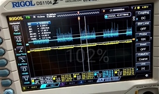
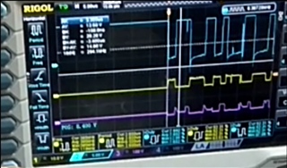
  • During testing, I encountered the following issues:

            1.The integrated circuit (IC) is getting damaged under both load and no-load conditions.
            2.When I increase the voltage, the IC heats up and eventually gets damaged.


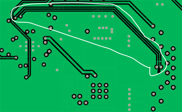
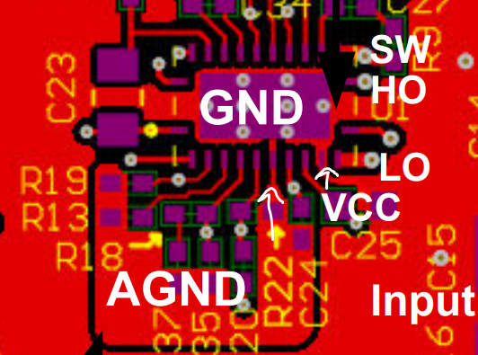
I have attached my schematic for your reference. 

I am seeking suggestions for improvement and kindly request your support in resolving this issue. 

RM-004-V-00.SchDoc

  • Sanjana,

    Please print out your schematic with the components you used on the real board, I'm sure some of your components are DNP.

    Also please attach quickstart calculator for this.

    https://www.ti.com/tool/download/SNVR504 

    Are you using VCCX? What does your layout look like?

    Maybe attach your altium project so I can review your layout then.

    -Orlando


  • I have provided you with the schematic, and below, I am attaching the PCB layout for your reference. While conducting practical experiments on my actual board, I have established the following connections. To observe these connections, please refer to my schematic.

    1. VCCX is connected to GND through a 0-ohm resistor at R18.

    2. PFM/SYNC is connected to GND through a 0-ohm resistor at R24.

    3. R1 is not connected.

    4. C1 and R3 is not connected.

    5. PG/SYNCOUT is connected to VCC through a 100K pullup resistor and a 0-ohm resistor instead of an LED.

    6.  R31 and R33 not connected.

    Please take note of the component values I am using:

    Q1, Q2: IAUC28N08S5L230ATMA1_1
    Q3, Q4: IAUC70N08S5N074ATMA1

    RM-004-V-00.PcbDoc

  • Sanjana,

    Note your Q3, and Q4 are not logic-level MOSFETs.

    They should be logic-level (VGS = 4.5V in datasheet), because LM5148 gate drive is only 5V.

    You should not be using VCCX and current sense VOUT on the same trace.

    Current sense VOUT needs to be kelvin routed with IOUT, this is a differential, noise sensitive signal.

    Also do not share this current sense VOUT with VCCX. 

    See LM25149-Q1EVM-2100 example.

    Your AGND needs to connect to PGND. This is usually done right by AGND pin and the exposed pad. 

    I'm confused why your PGND pin does not connect to Exposed pad either.

    See layout example.

    Can you confirm the converter is stable at no-load? Also what about no-load FPWM?

    Let me know,

    -Orlando


  • The converter exhibits instability under both loaded and unloaded conditions, and FPWM is not generated in either case.

    To address the incorrect traces on my PCB causing this issue, what steps can I take to rectify the problem?

    Is it feasible to use the same Q1 and Q2 MOSFETs for Q3 and Q4 as well?

  •  I am using the LM5149-Q1 Buck Converter Evaluation Module User's Guide and the evaluation board LM5149-Q1EVM-400 (BSR170) . Is it ok to refer it?

  • Sanjana,

    LM5149-Q1EVM-400 is good to reference as well yes, you can see the differential current sense routing on that as well, and the dedicated current sense trace.

    It would be best to re-spin the board with updated layout yes.

    On your existing board, you can try to swap the standard level FETs to logic level FETs yes. 

    I didnt realize you had R7 to connect AGND to PGND.

    -Orlando

  • Hi,

    I have implemented the alterations in my PCB based on your guidelines. The waveform generated at the gate of high and low side MOSFET, as depicted in the attached image of the PWM waveform, is not accurate. Kindly examine and provide guidance on potential issues with my PCB.

    The image below illustrates the PWM waveform. In this depiction, the yellow waveform represents the gate of the low-side MOSFET, while the blue waveform corresponds to the gate of the high-side MOSFET. 


    I made some changes to fix the above ringing problem(refer the schematic provided to you):

    I switched C39 to 200nF.
    I set R11 to 25 ohms.
    Now, the waveform looks different (waveform 1). Take a look and let me know if these changes helped reduce the ringing issue. 

    In this depiction,  waveform 1 represents the gate of the high-side MOSFET, waveform 2 corresponds to the gate of the low-side MOSFET, waveform 3 is of switching pin of IC.

  • Hello, The responsible engineeer is out of office now. TI responses may be delayed during the end year Holiday Season until Jan 2nd, 2024. Thank you for your patience.

  • Hello Sir, I am waiting for your reply. please reply if your concern person is back.

  • Hello ,

    Kindly review the following PCB layout and updated Schematic I have made changes as per your guidlines if any updates in that please suggest me. will you please share your maiRM-004-V-00.rarl ID? so we can properly communicate regarding this issue.

  • Sanjana,

    Your schematic looks great.

    The layout looks good as far as two-layer and 0805 components can get.

    Of course smaller 0603 and even 0402 components will allow better layout for small signal components around the IC.

    I'd say maybe connect PGND pin 10 to the LM5148 exposed pad also.

    Also VOUT trace to R31 is better to tie to CON3 or TP5, instead of trace from output capacitor.

    Maybe add more GND vias by output capacitor C22 and C29. You can also add more GND vias to Q3 and Q4 with smaller annular rings, like the vias you use for high-side FETs.

    Hope this helps,

    -Orlando

  • Hello Sir ,


    Thank you for your guidance, sir. I have incorporated the changes you recommended and updated my PCB layout. Please review the revised PCB layout.

    6038.RM-004-V-00.PcbDoc

  • Sanjana,

    Looks good. I am not sure what you have two unconnected traces/tracks but its fine I guess.

    Hope this helps,

    -Orlando